Learning Outcomes
- Explain the need for forced commutation in SCR-based inverters and describe the McMurray half-bridge turn-off sequence.
- Draw and label the three-phase full-bridge IGBT VSI circuit, identifying all switch pairs and freewheeling diodes.
- State the purpose of the DC bus capacitor and explain dead-time compensation.
- Construct the six-step gating table and deduce the resulting pole and phase voltage waveforms.
- Compute the fundamental and harmonic voltages of the six-step inverter using its Fourier expansion.
- Explain how harmonic currents cause motor derating and identify the dominant harmonic orders and their phase sequence.
SCR Inverters: Forced Commutation
- SCRs (thyristors) turn ON via a gate pulse but cannot be turned OFF via the gate — they commutate off only when anode current falls below the holding current \(I_H\)
- In a DC-link inverter the load current never naturally reverses → external forced commutation is required
- Solution: auxiliary \(LC\) resonant circuit — the Modified McMurray half-bridge
Commutation Component Sizing
Constraint: \(t_q \geq t_{q,\min}\) from the SCR datasheet. \(t_q\) is the SCR turn-off (circuit-commutated recovery) time.
- Step 1: Auxiliary SCR \(T_{1A}\) gated ON; commutation capacitor \(C_c\) resonantly charges via \(L_c\) to approximately \(2V_{dc}\)
- Step 2: \(C_c\) voltage reverse-biases \(T_1\); reverse voltage is maintained for the duration \(t_q \geq t_{q,\min}\)
- Step 3: \(T_1\) turns OFF; load current transfers to the \(L_c\)–\(C_c\) resonant path
- Step 4: Freewheeling diode \(D_1\) conducts; residual energy in \(L_c\) is returned to \(+V_{dc}\)
- Step 5: \(T_2\) (complementary switch) assumes full load current; \(C_c\) resets for the next commutation event
| Feature | SCR | IGBT |
|---|---|---|
| Turn-off method | \(LC\) resonance (forced) | Gate signal (self) |
| Switching frequency | <500 Hz | 1–20 kHz |
| Auxiliary parts | Required (\(L_c\), \(C_c\), auxiliary SCR) | None |
| Control effort | High; complex timing | Low; simple gate drive |
| Audible noise | High (<500 Hz switching) | Low (>1 kHz) |
The IGBT Revolution
- IGBT: combines a voltage-controlled MOSFET gate with low-saturation-voltage BJT conduction path
- Freely turned ON and OFF by gate voltage alone — no resonant commutation circuit
- Eliminates \(L_c\), \(C_c\), and auxiliary SCRs → component count reduced by ~60%
- Switching frequency: 1–20 kHz vs. <500 Hz for forced-commutated SCR
- Dramatically reduces audible noise, physical size, and drive complexity
- Enables high-quality PWM output — the subject of Lecture 7E
| Era | Key Development |
|---|---|
| 1960s–70s | SCR forced-commutation inverters |
| 1980s | GTO devices; simpler commutation |
| 1990s | IGBT revolution; PWM at kHz rates |
| 2000s+ | DSP control; SVM; field orientation |
| Today | SiC/GaN; >100 kHz switching; higher efficiency |
Why Study the McMurray Circuit?
SCR inverters are now obsolete in most drives. Studying the McMurray circuit establishes the principles of forced commutation and explains why fully self-commutating devices (IGBT, GTO, IGCT) fundamentally transformed power electronics. It also provides context for understanding CSI drives (Lecture 7F), where commutation principles remain relevant for thyristor-based designs.
Three-Phase IGBT Full-Bridge VSI: Circuit Structure
- 6 IGBT switches, each with an anti-parallel freewheeling diode
- Upper group: \(T_1\) (phase \(a\)), \(T_3\) (phase \(b\)), \(T_5\) (phase \(c\))
- Lower group: \(T_4\) (phase \(a\)), \(T_6\) (phase \(b\)), \(T_2\) (phase \(c\))
- Complementary pairs: \(T_1 \leftrightarrow T_4\), \(T_3 \leftrightarrow T_6\), \(T_5 \leftrightarrow T_2\)
- Dead time (1–4 µs) inserted between complementary gate signals to prevent DC bus short-circuit (shoot-through)
Voltage Equations (DC midpoint O)
Pole voltages take values \(\{+V_{dc}/2,\;-V_{dc}/2\}\):
Phase voltage referred to load neutral \(N\):
This formula eliminates the zero-sequence (common-mode) component, giving the true phase-to-neutral voltage of a balanced three-phase load.
Why Freewheeling Diodes Are Essential:
- Motor is an inductive load: phase current cannot change instantaneously
- When an IGBT turns off, the inductor drives current to continue in the same direction
- Freewheeling diodes provide the necessary current path, preventing open-circuit conditions
- Without them: stray inductance generates destructive over-voltage spikes across the IGBTs
Required DC Bus Voltage — Example (415 V motor)
For six-step VSI, the fundamental peak phase voltage is:
Diode-rectified 415 V (L-L) gives \(V_{dc} \approx \sqrt{2} \times 415 = 587\) V, which is above the 532 V needed — confirming the diode rectifier is adequate.
DC Bus Capacitor & Dead-Time Compensation
- Large electrolytic capacitor \(C_f\) across the DC bus maintains a stiff \(V_{dc}\) despite pulsating inverter currents
- Absorbs regenerated energy during motor braking (works with braking chopper + resistor)
- Typical sizing: approximately 100 µF per kW of drive rating
- Also absorbs high-frequency switching ripple current — choose low-ESR (Equivalent Series Resistance) type for long service life
Braking Chopper + Resistor Operation
During deceleration, kinetic energy returns to \(C_f\), raising \(V_{dc}\). When \(V_{dc}\) exceeds a threshold, a chopper transistor switches a braking resistor across the bus, dissipating the excess energy as heat. With an Active Front-End (AFE), energy is returned to the supply instead — a more efficient solution for frequent braking applications.
Dead time prevents shoot-through but also distorts the output voltage by amplifying low-order odd harmonics and introducing a fundamental voltage magnitude error.
The peak fundamental voltage error per phase is approximately:
where \(t_{dead}\) is the dead time (s), \(f_{sw}\) is the switching frequency (Hz), and \(V_{dc}\) is the DC bus voltage (V).
Dead-Time Compensation Method
Measure phase current polarity at each switching instant and add or subtract \(\Delta\hat{V}_{as}\) to the voltage reference command. This is essential in high-performance drives operating at low speed (where \(f_{sw}/f_s\) is large) because dead-time error then represents a significant fraction of the commanded voltage.
Typical Dead-Time Values
IGBT drives: \(t_{dead}\) = 1–4 µs. At 10 kHz switching, this is 1–4% of a switching period, corresponding to a fundamental voltage error of approximately 2–8% of \(V_{dc}\).
Six-Step (180°) Operation
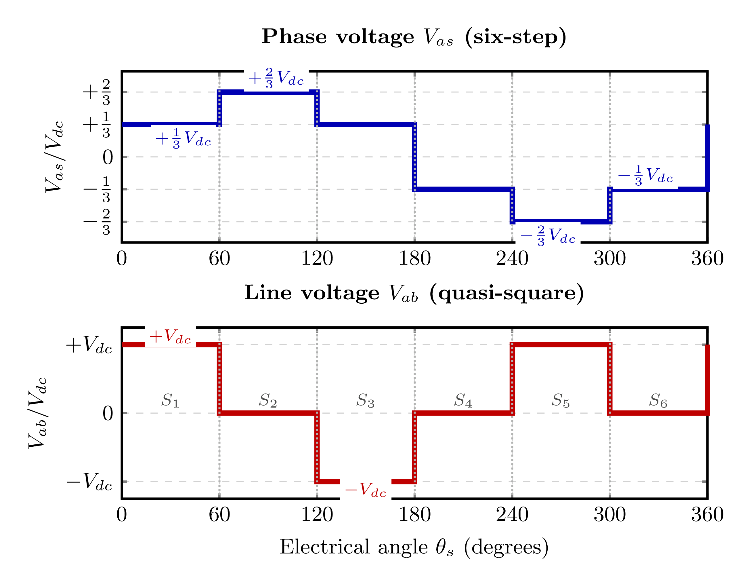
| Interval | Switches ON | Range | \(V_{as}/V_{dc}\) |
|---|---|---|---|
| I | \(T_1, T_5, T_6\) | \(0°–60°\) | \(+1/3\) |
| II | \(T_1, T_2, T_6\) | \(60°–120°\) | \(+2/3\) |
| III | \(T_1, T_2, T_3\) | \(120°–180°\) | \(+1/3\) |
| IV | \(T_2, T_3, T_4\) | \(180°–240°\) | \(-1/3\) |
| V | \(T_3, T_4, T_5\) | \(240°–300°\) | \(-2/3\) |
| VI | \(T_4, T_5, T_6\) | \(300°–360°\) | \(-1/3\) |
- Phase voltage \(V_{as}\) takes six distinct levels: \(\pm\tfrac{2}{3}V_{dc}\) and \(\pm\tfrac{1}{3}V_{dc}\) — hence the name "six-step"
- Line voltage \(V_{ab}\): quasi-square wave (\(+V_{dc}\), 0, \(-V_{dc}\))
Phase Voltage Fundamental (peak)
This is the amplitude of the fundamental sinusoidal component of the six-step phase voltage waveform.
Line Voltage Fundamental (peak)
The line voltage fundamental is \(\sqrt{3}\) times the phase voltage fundamental, as expected in a balanced three-phase system.
Harmonic Spectrum of the Six-Step VSI
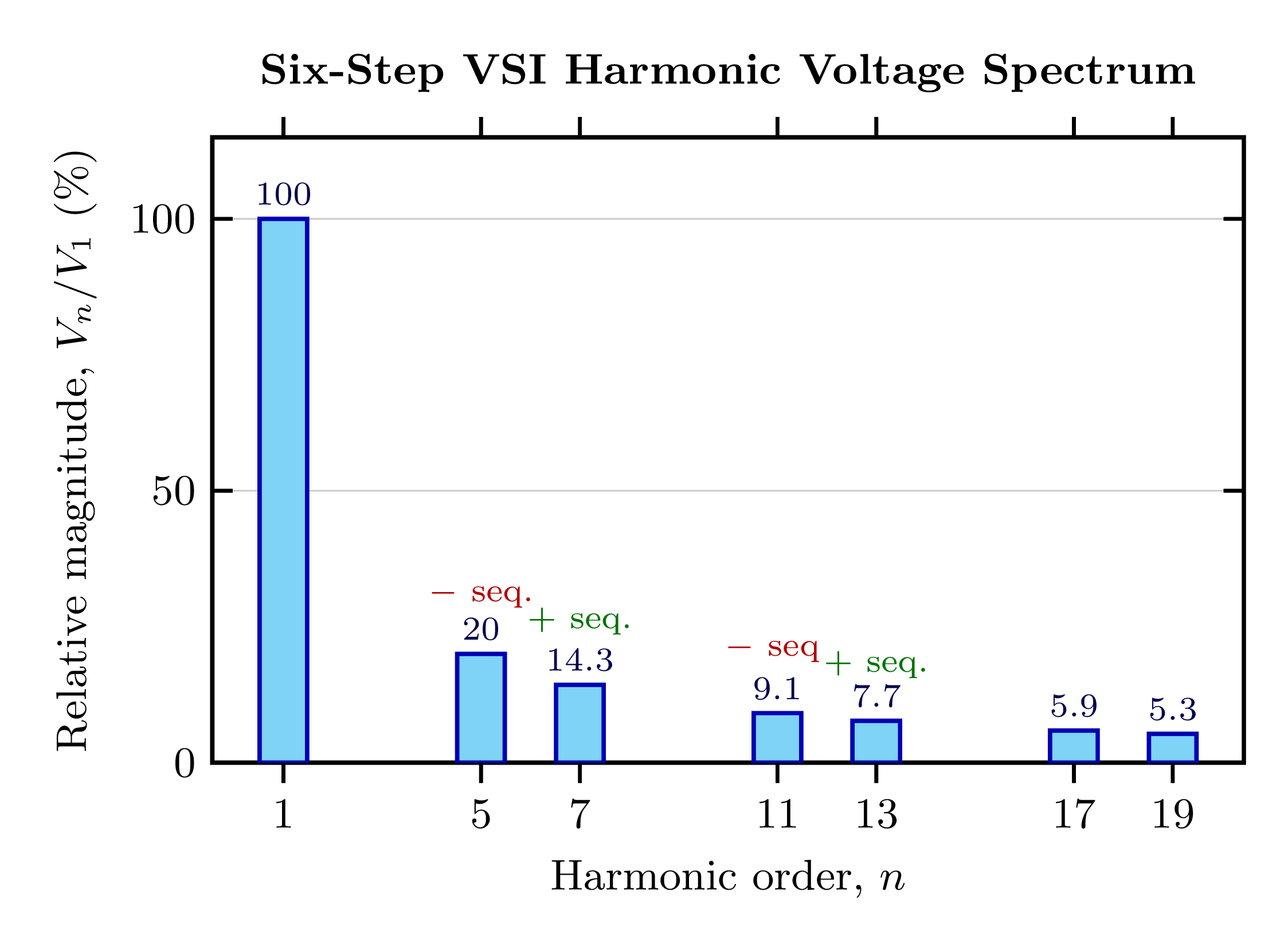
- Odd harmonics only (half-wave and quarter-wave symmetry)
- Triplen harmonics (3rd, 9th, 15th, …) cancel in balanced three-phase line voltages
- Remaining dominant orders: \(n = 6k \pm 1\), i.e., 5th, 7th, 11th, 13th, …
Harmonic Magnitudes
\(V_n/V_1 = 1/n\), so \(V_5 \approx 0.2\,V_1\) (20%) and \(V_7 \approx 0.143\,V_1\) (14.3%).
\(n = 6k-1\): negative sequence | \(n = 6k+1\): positive sequence
Voltage THD of Six-Step VSI
This is well above the IEEE 519 line harmonic limit of 5%, necessitating PWM techniques (Lecture 7E).
- 5th harmonic (negative sequence): produces backward-rotating air-gap flux → parasitic braking torque and extra rotor copper loss
- 5th and 7th together: produce torque ripple at \(6\omega_s\) — typically 6× the fundamental frequency. For a 50 Hz supply this is 300 Hz ripple.
- 11th and 13th: produce torque ripple at \(12\omega_s\)
- Harmonics raise both copper losses and core losses → extra heating in stator and rotor
- Motor is typically derated by ~10% when fed from a six-step VSI (per IEEE Std 112)
Remedy: PWM Techniques
PWM strategies (Lecture 7E) shift harmonics to high-frequency sidebands around the carrier \(f_c\). Motor leakage inductance then filters them effectively, yielding near-sinusoidal current. Motor derating is reduced from ~10% to ~1–3%, and torque ripple at \(6\omega_s\) is essentially eliminated.
| \(n\) | \(I_n/I_1\) | Sequence |
|---|---|---|
| 1 | 1.000 | Positive (forward) |
| 5 | 0.200 | Negative (backward) |
| 7 | 0.143 | Positive (forward) |
| 11 | 0.091 | Negative (backward) |
| 13 | 0.077 | Positive (forward) |