Field-effect transistor (FET)s
Introduction
Transistors are essential semiconductor devices.
Two major types:
Bipolar Junction Transistor (BJT)
Field-Effect Transistor (FET)
BJTs use both electrons and holes (bipolar)
FETs use only one type of charge carrier (unipolar).
What is a Field-Effect Transistor (FET)?
A voltage-controlled semiconductor device.
Controls current flow using an electric field.
Two main types:
Junction Field-Effect Transistor (JFET)
Metal-Oxide Semiconductor Field-Effect Transistor (MOSFET)
BJT vs. FET
| Feature | BJT | FET |
|---|---|---|
| Charge Carriers | Electrons & Holes (Bipolar) | Electrons or Holes (Unipolar) |
| Control Mechanism | Current-Controlled | Voltage-Controlled |
| Input Impedance | Low | High |
| Switching Speed | Slower | Faster |
| Preferred Applications | Amplifiers | Switching & High Impedance Circuits |
Junction Field-Effect Transistor (JFET)
Consists of three terminals: Gate, Source, and Drain.
Operates with reverse-biased pn junction to control current in a channel.
Two types based on channel structure:
N-channel JFET: Current flows through an n-type channel.
P-channel JFET: Current flows through a p-type channel.
High input impedance, making it useful in high-impedance amplifiers.

Basic Operation of JFET
Reverse-biased gate-source junction controls current flow.
\(V_{DD}\) provides drain-to-source voltage, allowing current flow from drain to source.
\(V_{GG}\) sets reverse-bias voltage, producing a depletion region along the pn junction.
The depletion region controls channel width and resistance.
Wider depletion region towards the drain end due to greater reverse-bias voltage.

JFET Characteristics and Parameters
Voltage-Controlled Device: JFET operates as a voltage-controlled, constant-current device.
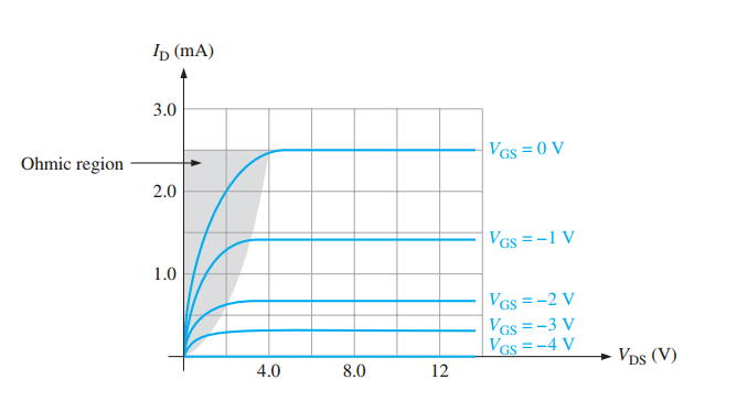
Drain Characteristic Curve:
\(I_D\) increases with \(V_{DS}\) initially (Ohmic region) but becomes constant in the active region.
Pinch-off voltage (\(V_p\)) is where \(I_D\) becomes constant.

Breakdown Region:
Occurs when \(I_D\) increases rapidly beyond safe limits.
JFET must be operated below breakdown voltage.
\(V_{GS}\) Controls \(I_D\):
Increasing negative \(V_{GS}\) reduces \(I_D\) due to narrowing of the channel.
The cutoff voltage (\(V_{GS}\text{(off)}\)) is where \(I_D\) is approximately zero.
For an n-channel JFET, the more negative \(V_{GS}\) is, the smaller \(I_D\) becomes.
\(V_{GS}\)(off) and \(V_p\) are equal in magnitude but opposite in sign.

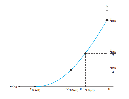
JFET Universal Transfer Characteristic
Transfer characteristic curve: \(V_{GS}\) and \(I_{D}\) relationship.
Also known as the transconductance curve.
Key characteristics:
\(I_{D} = 0\) when \(V_{GS} = V_{GS(off)}\)
\(I_{D} = I_{DSS}\) at \(V_{GS} = 0\)
\(I_{D}\) follows a square-law relationship:
\(I_{D}\) can be determined for any \(V_{GS}\) if \(V_{GS(off)}\) and \(I_{DSS}\) are given.
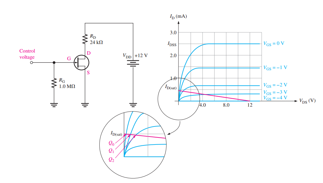
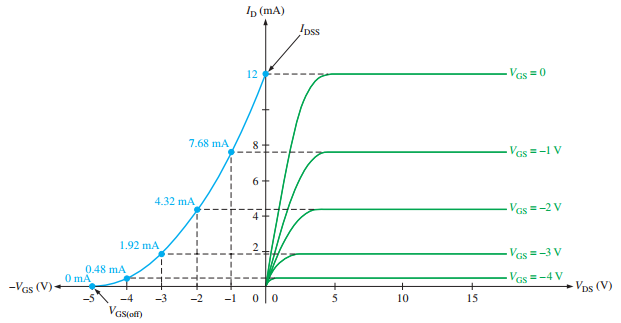
An example of how the transfer characteristic curve (blue) of an n-channel JFET is developed from the JFET drain characteristic curves (green).
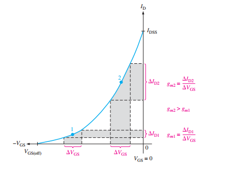
JFET Forward Transconductance
- \(\Delta V_{GS}\)\(\Delta I_D\)Forward Transconductance (g\(_m\)):\[\begin{aligned} g_m & = \frac{\Delta I_D}{\Delta V_{GS}} \\ g_m & = g_{m0} \left(1 - \frac{V_{GS}}{V_{GS(off)}} \right)\\ g_{m0} &\Rightarrow~ \text{transconductance at}~ V_{GS} = 0 \end{aligned}\]
- is unknown, it can be estimated as: When\[g_{m0} = \frac{2 I_{DSS}}{|V_{GS(off)}|}\]
JFET has high input resistance (\(R_{IN}\)) due to reverse-biased gate-source junction.
\[R_{IN} = \left| \frac{V_{GS}}{I_{GSS}} \right|\]Input Capacitance (C\(_{iss}\)): Results from the reverse-biased pn junction.
AC Drain-to-Source Resistance (r\(_{ds}'\)): Resistance in the active region where \(I_D\) remains constant over a range of \(V_{DS}\).
\[r_{ds}' = \frac{\Delta V_{DS}}{\Delta I_D}\]Often specified in terms of output conductance \(g_{os}\).
JFET Biasing
The purpose of biasing is to set a proper Q-point.
Three types of biasing in the active region:
Self-bias
Voltage-divider bias
Current-source bias
Self-Biasing
Ensures gate-source junction is reverse-biased.
\[\begin{aligned} V_{GS} &= -I_D R_S \Leftarrow \text{n-channel JFET}\\ V_{GS} &= +I_D R_S \Leftarrow \text{p-channel JFET} \end{aligned}\]
Biasing at the midpoint allows maximum current swing.
The Q-point is determined by plotting the load line.
- The load line equation:\[V_{GS} = -I_D R_S\]
Intersection of load line and transfer characteristic gives \(I_D\) and \(V_{GS}\).