Bipolar Junction Transistor (BJT) Power Amplifiers
Power Amplifiers: Overview & Classification
Input Signal: Small, amplified to use full load line.
Stages:
Small-signal transistors: \(<\) 1 W, used in early stages (low power).
Power transistors: \(>\) 1 W, used in final stages (high power).
Load Impedance: Lower at later stages, e.g., stereo speakers (\(8~\Omega\) or less).
Voltage Amplifier Vs Power Amplifier

Large-Signal Amplifiers
Use a large portion of load line.
Classes:
Class A: 100% of the input cycle in the linear region.
Class B: 50% cycle.
Class AB: Between 50%–100%.
Class C: \(<\) 50%.
Applications
Final stage of communication systems (receivers/transmitters).
Provide power to speakers or antennas.
Example: BJTs illustrate power amplifier principles.
Amplifier Terms
Classification by Operation:
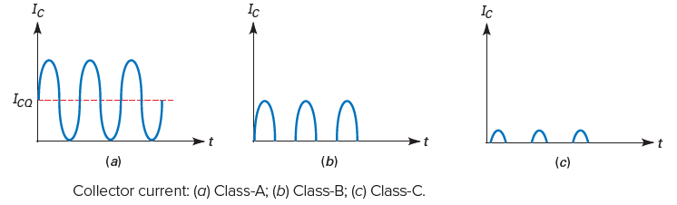
Class A: Collector current flows for 360° of AC cycle.
Class B: Collector current flows for 180° (Q-point at cutoff).
Class C: Collector current flows for \(<\) 180° of AC cycle.
Types of Coupling
Capacitive Coupling: Blocks DC, transmits AC.
Transformer Coupling: AC coupled through a transformer.
Direct Coupling: DC and AC connected directly between stages.

Frequency Ranges
Audio Amplifier: 20 Hz to 20 kHz.
RF Amplifier: Amplifies frequencies above 20 kHz (e.g., FM: 88–108 MHz).

Narrowband: Small range, tuned RF amplifiers (e.g., 450–460 kHz).
Wideband: Large range (e.g., 0–1 MHz).
Signal Levels
Small Signal: Swing \(<\) 10% of quiescent collector current.
Large Signal: Uses full load line.
Preamp: Picks up small signals, amplifies before passing to power amplifier.
Power Amplifier: Final stage, output power from milliwatts to hundreds of watts.
Two Load Lines: DC and AC
Amplifier Behavior:
DC and AC load lines intersect at the Q-point.
Q-point location is critical for maximum output in large-signal amplifiers.
DC Load Line
- Equation:\[I_{C(\mathrm{sat})} = \frac{V_{CC}}{R_C + R_E} \quad \text{(Saturation)}\]
Moves with changes in biasing (e.g., varying \(R_2\)).

AC Load Line
- \[\begin{aligned} I_C &= I_{CQ} + \frac{V_{CEQ}}{r_c} - \frac{V_{CE}}{r_c} \\ i_{c(\mathrm{sat})} &= I_{CQ} + \frac{V_{CEQ}}{r_c}~~\text{Saturation} \\ v_{ce(\mathrm{cutoff})} &= V_{CEQ} + I_{CQ} r_c~~\text{cut-off}\\ \end{aligned}\]
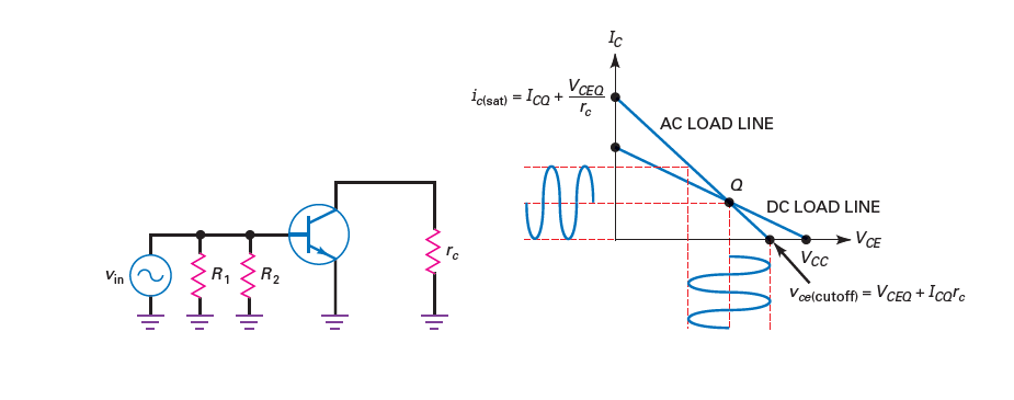
Maximum Peak-to-Peak Output (MPP) \(< V_{CC}\)
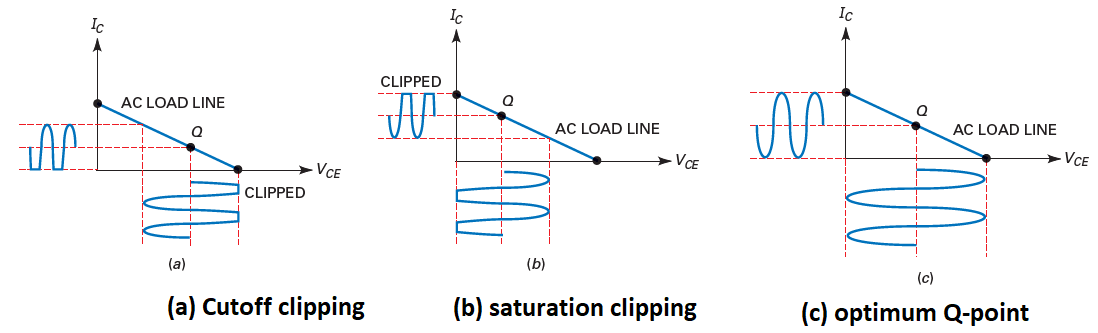
Clipping of Large Signals
Clipping Causes:
Cutoff Clipping: Q-point too low \(\rightarrow\) Signal driven into cutoff.
Saturation Clipping: Q-point too high \(\rightarrow\) Signal driven into saturation.
Both lead to signal distortion and poor sound quality.
Ideal Design:
Q-point at the middle of the AC load line \(\rightarrow\) Maximum unclipped output.
Unclipped peak-to-peak output is called AC output compliance.
Class A Power Amplifier
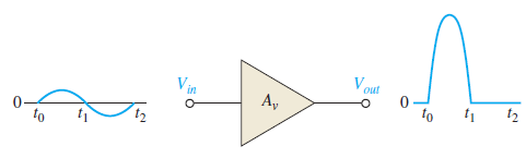
Definition: Biased to always operate in the linear region; output is an amplified replica of the input.
Power Amplifiers: Deliver power (rather than just voltage) to a load.
Rated \(>\) 1 W.
Heat dissipation must be considered.

Heat Dissipation
Power transistors must dissipate heat efficiently.
Collector Terminal: Connected to the case for heat transfer.
Heat Sinks: Vary in size, material, and design to manage heat.
High-power applications may require cooling fans.
Centered Q-Point
Q-Point Location: center of the AC load line for max. output signal.
Collector Current (\(I_{CQ}\)): Varies from \(I_{C(sat)}\) to 0.
Collector-Emitter Voltage (\(V_{CEQ}\)): Varies from \(V_{CE(cutoff)}\) to near zero.
Clipping occurs if Q-point moves away from center (cutoff or saturation).

Power Gain
- Definition:\[A_p = \frac{P_L}{P_{in}}\]
- Formulas:\[P_L = \frac{V_L^2}{R_L} \quad \text{and} \quad P_{in} = \frac{V_{in}^2}{R_{in}}\]
- \(A_v = 1\)\(R_L = 100 \, \Omega\)\(R_{in} = 5 \, \text{k}\Omega\)Example (Common-Collector Amplifier):\[A_p = \left( 1^2 \right) \times \frac{5000}{100} = 50\]
DC Quiescent Power
- Formula:\[P_{\text{DQ}} = I_{\text{CQ}} V_{\text{CEQ}}\]
Interpretation: This represents the power dissipated with no input signal.
The transistor must be rated for power exceeding \(P_{\text{DQ}}\).
Output Power
- RMS value: Maximum Peak Voltage Swing (Centered Q-Point):\[V_{c(\text{max})} = I_{\text{CQ}} R_c\]
- RMS value: Maximum Peak Current Swing:\[I_{c(\text{max})} = \frac{V_{\text{CEQ}}}{R_c}\]
- Maximum Output Power:\[P_{\text{out(max)}} = 0.5 I_{\text{CQ}} V_{\text{CEQ}}\]
Efficiency
- Definition:\[\eta_{\text{max}} = \frac{P_{\text{out}}}{P_{\text{DC}}}\]
- DC Power Supply:\[P_{\text{DC}} = I_{\text{CC}} V_{\text{CC}} = 2 I_{\text{CQ}} V_{\text{CEQ}}\]
- Maximum Efficiency for Capacitively Coupled Class A Amplifier:\[\eta_{\text{max}} = \frac{0.5 I_{\text{CQ}} V_{\text{CEQ}}}{2 I_{\text{CQ}} V_{\text{CEQ}}} = 0.25 \quad \text{(25\%)}\]
Typical Efficiency: 10%
Transformer coupling improves efficiency but has drawbacks like size, cost, and potential distortion.
Class B and Class AB Amplifiers
Class B Amplifier:
Biased at cutoff, conducts for half the input cycle.
In cutoff for the other half.
More efficient than Class A, but causes crossover distortion.
Class AB Amplifier:
Biased above cutoff, conducts for \(\mathbf {200-220^\circ}\).
Reduces crossover distortion, more efficient than Class A.
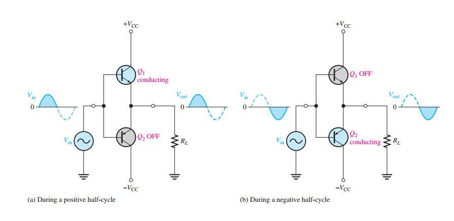
Push-Pull Configuration:
Two transistors: one for the positive, one for the negative half-cycle.
Enhances efficiency and power handling, requires proper biasing.
Comparison of Amplifier Classes

Class B Operation
- Basic class B amplifier operation (noninverting)
Transistor conducts only during one half-cycle.
Output is not an exact replica due to one half-cycle amplification.
No power dissipation when there is no input, except leakage currents.
Efficiency is much higher than Class A (up to 78.5%).
- Class B amplifier commonly uses push-pull emitter-follower
circuit.

In push-pull, one transistor amplifies the positive half-cycle, the other the negative.
Crossover distortion occurs due to a brief moment when neither transistor conducts at zero volts.
Class AB biasing is used to pre-bias transistors above cutoff, reducing distortion.
Class B Push-Pull Operation
A Class B push-pull amplifier consists of two transistors.
Each transistor conducts for only one half of the input cycle.
This method significantly improves efficiency compared to Class A amplifiers.
It introduces challenges like crossover distortion.
Two Common Push-Pull Configurations
Transformer-Coupled Push-Pull Amplifier
Uses an input transformer to split the input signal into two equal but opposite signals.
Two NPN transistors amplify each half-cycle separately.
An output transformer recombines the two amplified halves into a full waveform.
Pros: Provides signal phase splitting.
Cons: Transformers add bulk, cost, and potential core saturation distortion.

Complementary-Symmetry Push-Pull Amplifier
Uses one NPN transistor for the positive half-cycle and one PNP transistor for the negative half-cycle.
Operates without an input transformer, simplifying the circuit.
Requires both positive and negative power supplies.
Pros: More compact, eliminates the need for bulky transformers.
Cons: Susceptible to crossover distortion.
Crossover Distortion
Transistors stay off until input exceeds base-emitter threshold (\(V_{BE} \approx 0.7V\) for BJTs).
A small gap in the output occurs when neither transistor conducts.
This non-linearity causes distortion, especially in audio applications.

Class AB amplifiers slightly pre-bias the transistors to conduct for small input signals.
This reduces crossover distortion while maintaining high efficiency.
Class AB Biasing to Reduce Crossover Distortion
Designed to eliminate crossover distortion.
Achieved by slightly biasing the transistors into conduction even when no input signal is present.
Ensures that both transistors are never fully off at the same time.
Biasing with Diodes
Diodes D1 and D2 provide a voltage drop matching the transistors’ base-emitter junctions (\(V_{BE} \approx 0.7V\)).
This pre-biases both transistors into slight conduction, avoiding the dead zone in Class B operation.
Current Mirror Effect: If thermally matched, the diodes’ current remains stable.
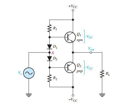
- that flows in Class AB mode is given by: The small\[I_{CQ} = \frac{V_{CC} - 0.7V}{R_1} ~~ (R_1~ \text{sets the biasing level})\]
Thermal Runaway and Stability
Problem: If transistors heat up, their \(V_{BE}\) drops, leading to higher conduction, causing more heat \(\rightarrow\) thermal runaway.
Solution:
Place diodes close to the transistors for thermal tracking.
Add small emitter resistors to stabilize current.
AC Operation and Load Line Analysis
Q-Point Placement:
In Class B, the Q-point is at cutoff (\(I_{CQ} = 0\)).
In Class AB, the Q-point is slightly above cutoff to prevent crossover distortion.
- This is the maximum collector current during full signal operation.AC Saturation Current\[I_{c(sat)} = \frac{V_{CC}}{R_L}\]
Efficiency Considerations:
Class A: 25% max efficiency (low due to continuous conduction).
Class B: 79% max efficiency (due to transistors only conducting for half cycles).
Class AB: Compromise between Class A and Class B (moderate efficiency with low distortion).
Single-Supply Push-Pull Amplifier
It operates similarly to a dual-supply amplifier.
It uses one voltage source (\(V_{CC}\)) instead of two.
The key difference is how the biasing is set.
AC coupling is used to handle the DC shift.

Biasing at Mid-Supply (\(V_{CC}/2\)) and Capacitive Coupling Requirement
In a dual-supply amplifier, the output is biased at 0V, allowing equal positive and negative swings.
In a single-supply amplifier, the output is biased at \(\frac{V_{CC}}{2}\) to allow both positive and negative swings.
Why? This ensures a symmetrical signal range for both positive and negative variations.
Since the output sits at \(\frac{V_{CC}}{2}\), capacitors are used to block DC:
Input Coupling Capacitor:
Blocks the DC bias from affecting the signal source.
Allows only AC components of the signal to pass through.
Output Coupling Capacitor:
Blocks the DC component of \(\frac{V_{CC}}{2}\) from reaching the load.
Allows only the amplified AC signal to pass.
Voltage Swing in Practice
Ideal case: Output swings from 0V to \(V_{CC}\).
Real-world case: Output doesn’t fully reach these limits due to:
Saturation voltage (\(V_{CE(sat)}\)) of the transistors.
Voltage drops across internal resistances.
Advantages and Disadvantages
Advantages:
Works with a single power supply, making it more practical for many applications.
Eliminates the need for a negative voltage source.
Disadvantages:
Requires capacitive coupling, which can introduce low-frequency distortion.
The usable voltage swing is slightly lower than in a dual-supply amplifier.
Class B/AB Performance
- Maximum Output Power:\[\begin{aligned} P_{out} & = I_{out(rms)} \cdot V_{out(rms)} \\ I_{out(rms)} & = 0.707I_{out(peak)} = 0.707I_{c(sat)}\\ V_{out(rms)} & = 0.707V_{out(peak)} = 0.707V_{CEQ} \\ P_{out} & = 0.5I_{c(sat)}V_{CEQ}\\ P_{out} & = 0.25I_{c(sat)}V_{CC}~~(\because V_{CEQ} = V_{CC}/2)\\ \end{aligned}\]
- The current is a half-wave signal with an average value of half the peak current DC Input Power:\[P_{DC} = I_{CC}V_{CC}\]
- Efficiency:\[\begin{aligned} \eta & =\frac{P_{\text {out }}}{P_{\mathrm{DC}}} \\ P_{\text {out }} & =0.25 I_{c(\text { sat }} V_{\mathrm{CC}} \\ \eta_{\max } & =\frac{P_{\text {out }}}{P_{\mathrm{DC}}}=\frac{0.25 I_{c(\text { sat })} V_{\mathrm{CC}}}{I_{c(\text { sat })} V_{\mathrm{CC}} / \pi}=0.25 \pi \\ & \boldsymbol{\eta}_{\max }=\mathbf{79\%} \end{aligned}\]
- \(R_2\)\(R_1\)Input Resistance:\[\begin{aligned} R_{\text{in}} &= \beta_{ac} \left( r_e^{\prime} + R_E \right) \parallel R_1 \parallel R_2 \\ &= \beta_{ac} \left( r_e^{\prime} + R_E \right) \parallel R_1 \parallel R_2 ~~(\because R_E=R_L) \end{aligned}\]
Class C Amplifiers Key Characteristics
Class C amplifiers: Conduction for \(<180^\circ\) of input signal cycle.
Efficiency: Highly efficient.
Nonlinearity: Not suitable for audio/linear applications.
Usage: Primarily in RF circuits.
Signal correction: Uses resonant circuits for distortion.
Biased Below Cutoff: Transistor off for most of input cycle.
Short Conduction Time: Transistor on for small portion of positive cycle.
Nonlinear Amplification: Output is distorted, requires tuned circuit for sinusoidal output.
High Efficiency: Up to 90%, ideal for high-power RF transmission.
Common Applications:
RF transmitters (AM/FM broadcasting, communication systems)
Oscillators (generating stable RF signals)
Modulators (controlling high-frequency signals with low-frequency inputs)
Basic Class C Circuit & Waveform
Resistive Load Example: For conceptual understanding, impractical in real applications.
Waveform Behavior:
Base voltage is biased below cutoff with negative \(V_{BB}\).
Transistor turns on when input voltage exceeds base-emitter threshold.
Collector current (\(I_C\)) flows briefly each cycle.
Load Line Analysis:
When fully on, transistor reaches \(I_{C(sat)}\).
When off, collector voltage is at peak.

Power Dissipation in a Class C Amplifier
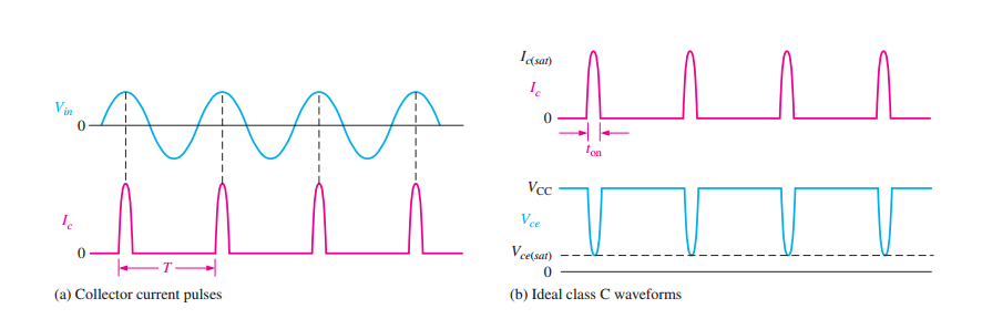
Collector Current Pulses
The transistor conducts only during short pulses in each input cycle.
The time between these pulses is the period \(T\) of the AC input voltage.
Voltage and Current During Conduction
During conduction:
The collector current reaches a peak of \(I_{c(sat)}\).
The collector-emitter voltage drops to \(V_{ce(sat)}\).
Power Dissipation Calculation
Power Dissipation During On-Time
Average Power Dissipation Over a Cycle
This shows that the lower the duty cycle (\(t_{\mathrm{on}}/T\)), the lower the average power dissipation, making class C amplifiers highly efficient.
Resistively Loaded Class C Amplifier
Unsuitable for Linear Applications
The output does not resemble the input signal.
Typical Usage
Class C amplifiers are used with a parallel resonant circuit (tank circuit).
Achieves Sinusoidal Output
The tank circuit shape the output into a sinusoidal waveform.

Resonant Frequency of the Tank Circuit
- The resonant frequency of the LC tank circuit is given by:\[f_r = \frac{1}{2\pi \sqrt{LC}}\]
At this frequency, the impedance of the tank circuit is highest, resulting in a large voltage gain.
How the Tank Circuit Produces a Sinusoidal Output
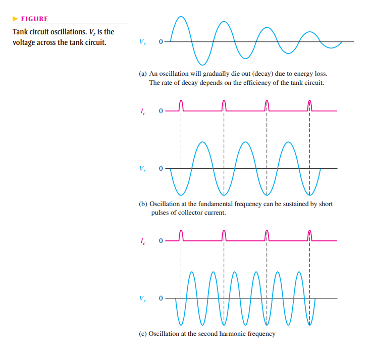
Initiation of Oscillation: A short pulse of collector current charges the capacitor to approximately \(+V_{CC}\).
Oscillation Cycle:
Capacitor discharges \(\rightarrow\) Inductor charges (magnetic field builds up).
Inductor’s magnetic field collapses \(\rightarrow\) Capacitor recharges in the opposite polarity.
This forms one complete cycle of oscillation.
Sustaining the Oscillation: Energy losses in the tank circuit’s resistance cause oscillations to die out, but each collector current pulse re-energizes the circuit, maintaining constant amplitude oscillations.

Frequency Multiplication Using Class C Amplifiers
If the tank circuit is tuned to the fundamental frequency, it oscillates at the input signal frequency.
If tuned to the second harmonic, it oscillates at twice the \(f_{in}\).
Higher harmonics can achieve further frequency multiplication.
Key Takeaways
Class C amplifiers are highly efficient but inherently nonlinear.
The LC tank circuit filters and converts the pulsed current into a sinusoidal output.
Frequency multiplication can be achieved by tuning the tank circuit to a harmonic frequency.
Maximum Output Power and Efficiency
- \(R_c\), and the maximum output power is: The tank circuit voltage has a peak-to-peak value of about\[P_{\text{out}} = \frac{V_{\text{rms}}^2}{R_c} = \frac{(0.707 V_{\mathrm{CC}})^2}{R_c} = \frac{0.5 V_{\mathbf{CC}}^2}{R_c}\]
- The total power supplied to the amplifier is:\[P_{\mathrm{T}} = P_{\text{out}} + P_{\mathrm{D}(\mathrm{avg})}\]
- ) is given by: The efficiency (\[\eta = \frac{P_{\text{out}}}{P_{\text{out}} + P_{\mathrm{D}(\text{avg})}}\]
When \(P_{\text{out}} \gg P_{\mathrm{D}(\text{avg})}\), \(\eta \approx~1 \Rightarrow 100\%\).
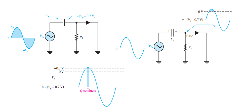
Bias Clamping Action in Class C Amplifiers
Clamping Circuit: Used in Class C amplifiers.
Function: Biases the transistor at a negative voltage level.
Operation: Transistor conducts only at the positive peaks of the input signal.
Effect: Ensures the transistor is turned on during positive cycles and off during negative cycles of the input.

Working of the Clamping Circuit
Charging of Capacitor \(C_1\) (During Positive Peak)
When the input signal goes positive, capacitor \(C_1\) charges to \(V_p - 0.7V\) through the base-emitter diode.
This establishes a negative average DC voltage at the transistor’s base (\(-V_p\)).
Maintaining the Charge (Large RC Time Constant)
The capacitor discharges very slowly because the \(R_1C_1\) time constant is much greater than the period of the input signal.
As a result, the average charge on the capacitor remains close to \(V_p - 0.7V\).

Establishing the Base Voltage
Since the DC value of \(V_{in}\) is 0V, the transistor base (negative side of \(C_1\)) sits at:
The AC input signal is superimposed on this DC level, shifting the \(V_B\) up and down accordingly.
Transistor Conducts Only at Positive Peaks
When input signal reaches its peak, \(V_B\) momentarily exceeds \(0.7V\).
This forward-biases the B-E junction, allowing the transistor to conduct briefly.