Demonstrative Video
Need for a Diode — Initial Thoughts
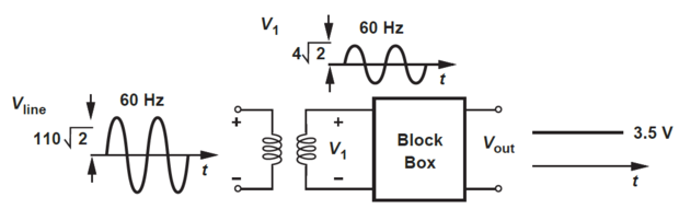
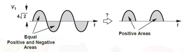
Signal Conversion Chain
- Output of the transformer using a black box exhibits a zero dc content — the negative and positive half-cycles enclose equal areas, leading to a zero average value.
- A diode eliminates the negative half-cycle to produce a non-zero average (DC) output.
DIODE — Basic Ideas
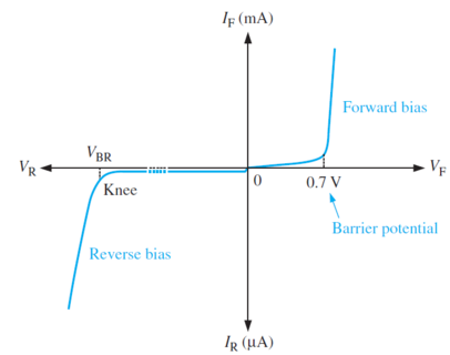
- Resistor \(\rightarrow\) linear device \(\rightarrow\) current vs voltage is a straight line.
- Diode \(\rightarrow\) nonlinear device \(\rightarrow\) \(I\) vs \(V\) is not a straight line.
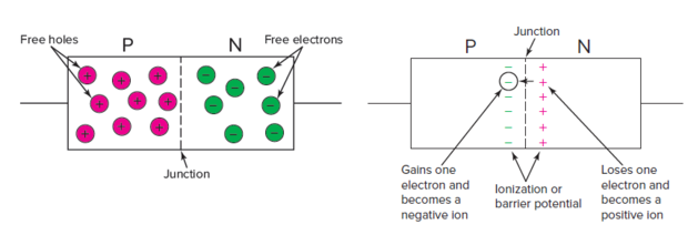
- The reason is the barrier potential.
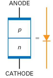
Definition
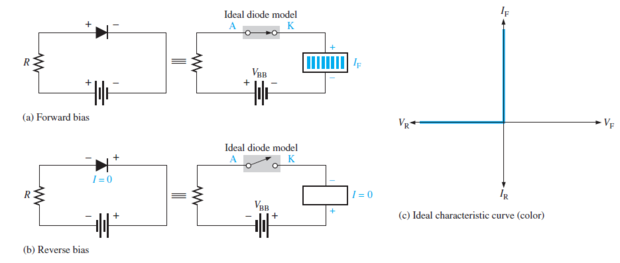
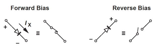
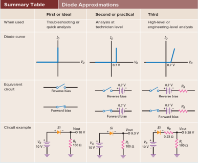
Ideal Diode: acts like a perfect conductor (zero resistance) when forward biased and like a perfect insulator (\(\infty\) resistance) when reverse biased.
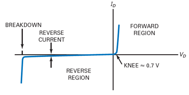
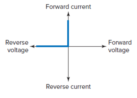
Diode Characteristic Curve
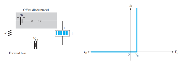
Real Diode
Ideal Diode
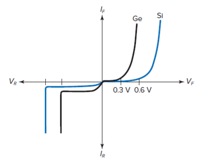
Si vs Ge
- Above the knee voltage, the diode current increases rapidly.
- A small increase in the diode voltage causes large increases in diode current.
-
Bulk Resistance:
\[R_B = R_p + R_n\]\(R_B\) is less than 1 Ω and depends on the size of the p and n regions and how heavily doped they are.
-
Maximum DC Forward Current: If the current in a diode is too large, the excessive heat can destroy the diode. The \(I_{F(\max)}\) is one of the maximum ratings given on a datasheet.
-
Power Dissipation:
\[\begin{aligned} P_D &= V_D \cdot I_D \\ P_{\max} &= V_{\max} \cdot I_{\max} \end{aligned}\]The power rating is the maximum power the diode can safely dissipate without shortening its life or degrading its properties.
Diode Current Equation
The diode current equation relating the voltage and current:
Key Result
-
When the diode is reverse biased, its current equation may be obtained by changing the sign of the applied voltage \(V\).
-
Thus, the diode current with reverse bias is:
\[I = I_o\left[\mathrm{e}^{\left(-V / \eta V_T\right)} - 1\right]\]
-
If \(V \gg V_T\), then the term \(\mathrm{e}^{(-V/\eta V_T)} \ll 1\), therefore \(I \approx -I_o\) — termed as reverse saturation current, which is valid as long as the external voltage is below the breakdown value.
Effect of Temperature
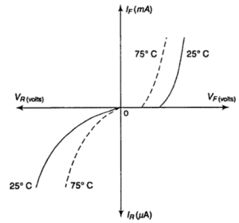
- \(T\uparrow \;\Rightarrow\;\) generation of electron–hole pairs increases, which increases the conductivities.
- If \(T\uparrow\) at fixed \(V \;\Rightarrow\; I\) increases.
- To bring \(I\) to normal \(\;\Rightarrow\; V\downarrow\).
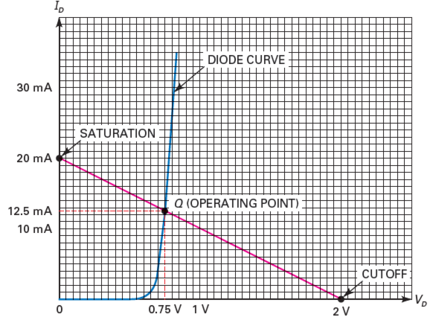
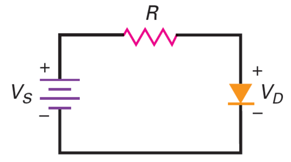
Load Lines
Load Line (KVL)
Load line: a straight line on the \(I_D\)–\(V_D\) plane whose intersection with the diode characteristic defines the Q-point.
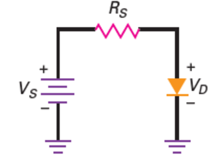
If \(V_s = 2~\mathrm{V}\), \(R = 100~\Omega\)
\(V_D = 0 \;\Rightarrow\; I_D = 20~\mathrm{mA}\)
\(I_D = 0 \;\Rightarrow\; V_D = V_s = 2~\mathrm{V}\)
The straight line is called the load line.
\(Q\) is an abbreviation for quiescent, which means "at rest."