Electronic Devices & Circuits · Lecture 23

Bipolar Junction Transistor (BJT)- Amplifiers

Bipolar Junction Transistors

Dr. Mithun Mondal BITS Pilani, Hyderabad Campus

Bipolar Junction Transistor (BJT)- Amplifiers

SECTION 01

Transistor Biasing and Small-Signal Amplifiers

  • Biasing of a transistor is purely a DC operation.

  • Purpose of biasing: Establish a Q-point for current and voltage variations in response to an AC input signal.

  • In applications requiring amplification of small signal voltages (e.g., from an antenna or microphone), variations around the Q-point are kept relatively small.

  • Amplifiers for these small AC signals are called small-signal amplifiers.

SECTION 02

Linear Amplifier Operation and Transistor Behavior

  • A linear amplifier amplifies a signal without distortion, providing an exact amplified replica of the input.

  • In a voltage-divider biased transistor:

    • Coupling capacitors \(C_1\) and \(C_2\) block DC, preventing changes in the bias voltages at the base and collector.

    • The capacitors appear as shorts to the signal voltage.

      image

  • Sinusoidal AC source causes base voltage to vary around the DC bias \(V_{BQ}\).

  • The base current variation leads to a larger variation in collector current due to transistor current gain.

  • Collector voltage decreases as the collector current increases, and vice versa.

  • The collector-to-emitter voltage varies out of phase with the base voltage.

  • Phase inversion: There is always a phase shift between base and collector voltage.

SECTION 03

Base Current and AC Load Line in a Linear Amplifier

image
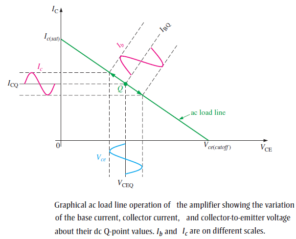
  • The sinusoidal voltage at the base produces a base current that varies above and below the Q-point along the AC load line.

  • Peak-to-peak variations in collector current and collector-to-emitter voltage are shown by lines projected from the peaks of the base current.

  • The AC load line differs from the DC load line:

    • The effective AC collector resistance is \(R_L\) in parallel with \(R_C\), which is less than the DC collector resistance \(R_C\) alone.

  • The distinction between the DC and AC load lines is explored further in the context of power amplifiers.

SECTION 04

Transistor Models in Amplifier Circuits

  • Purpose: Represent the operation of a transistor in an amplifier using a model circuit.

  • Transistor Model Circuit: Utilizes internal transistor parameters to describe operation.

  • Types of Parameters:

    • r Parameters: Based on resistance values, commonly used to model transistor behavior.

    • h Parameters: An alternative system of parameters, briefly discussed.

  • The five r parameters commonly used for BJTs are:
    image
SECTION 05

r-Parameter Transistor Model

image
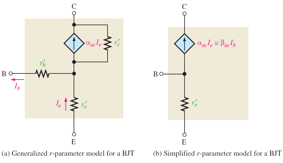
  • \(r_b^{\prime}\) is small enough to neglect \(\Rightarrow\) replaced by short

  • \(r_c^{\prime}\) usually several hundred \(\mathrm{k}\Omega\) \(\Rightarrow\) replaced by open

  • \(r_e^{\prime}\) is seen looking into the emitter of a F.B. transistor

  • Collector acts as a dependent current source of \(\alpha_{ac}I_e\) or \(\beta_{ac}I_b\)

  • \(r_e^{\prime}\) is the most important r-parameter

\[r_e^{\prime} \cong \dfrac{25~\mathrm{mV}}{I_E}\]
  • \[\begin{aligned} \beta_{dc} & = \dfrac{I_C}{I_B}\\ \beta_{ac} & = \dfrac{\Delta I_C}{\Delta I_B}\\ \end{aligned}\]
    \(I_B\)\(I_C\)
image
SECTION 06

h (hybrid) Parameters

image
SECTION 07

Common Emitter Amplifier

How Phase Inversion Occurs:

Conclusion

\[\begin{aligned} R_{\mathrm{TH}}&=\frac{R_{1}R_{2}}{R_{1}+R_{2}}\\ &=\frac{(6.8\mathrm{k}\Omega)(22\mathrm{k}\Omega)}{6.8\mathrm{k}\Omega+22\mathrm{k}\Omega}=5.19\mathrm{k}\Omega\\ V_{\mathrm{TH}}&=\left(\frac{R_2}{R_1+R_2}\right)V_{\mathrm{CC}}\\ &=\left(\frac{6.8\mathrm{k}\Omega}{6.8\mathrm{k}\Omega+22\mathrm{k}\Omega}\right)12\mathrm{V}=2.83\mathrm{V}\\ I_{\mathrm{E}}&=\frac{V_{\mathrm{TH}}-V_{\mathrm{BE}}}{R_{\mathrm{E}}+R_{\mathrm{TH}}/\beta_{\mathrm{DC}}}\\ &=\frac{2.83\mathrm{V}-0.7\mathrm{V}}{560\Omega+34.6\Omega}=3.58\mathrm{mA}\\ I_{\mathrm{C}}&\cong I_{\mathrm{E}}=3.58\mathrm{mA}\\ V_{\mathrm{E}}&=I_{\mathrm{E}}R_{\mathrm{E}}=(3.58\mathrm{~mA})(560\Omega)=2\mathrm{V}\end{aligned}\]
\[\begin{aligned} V_{\mathrm{B}} & =V_{\mathrm{E}}+0.7 \mathrm{~V}=2.7 \mathrm{~V} \\ V_{\mathrm{C}} & =V_{\mathrm{CC}}-I_{\mathrm{C}} R_{\mathrm{C}}=12 \mathrm{~V}-(3.58 \mathrm{~mA})(1.0 \mathrm{k} \Omega)=8.42 \mathrm{~V} \\ V_{\mathrm{CE}} & =V_{\mathrm{C}}-V_{\mathrm{E}}=8.42 \mathrm{~V}-2 \mathrm{~V}=6.42 \mathrm{~V} \end{aligned}\]

AC Signal Operation of an Amplifier

image

Signal (AC) Voltage at the Base

image

Input Resistance at the Base

\[\begin{aligned} R_{\text{in(base)}} &= \frac{V_{\text{in}}}{I_{\text{in}}} = \frac{V_b}{I_b} \\ V_b & = I_e r_e^{\prime} \\ I_e & \cong I_c \\ I_b &\approx \frac{I_e}{\beta_{\text{ac}}} \\ R_{\text{in(base)}} &= \frac{V_b}{I_b} = \frac{I_e r_e^{\prime}}{I_e / \beta_{\text{ac}}} \\ R_{\text{in(base)}} &= \beta_{\text{ac}} r_e^{\prime} \end{aligned}\]

Output Resistance of Common-Emitter Amplifier

Voltage Gain

\[\begin{aligned} A_v & =\frac{V_{out}}{V_{in}}=\frac{V_c}{V_b} \\ V_{c} & =\alpha_{ac}I_{e}R_{\mathrm{C}}\cong I_{e}R_{\mathrm{C}} \\ V_b & =I_{e}r_{e}^{\prime}\\ A_v & =\frac{I_eR_\mathrm{C}}{I_er_e^{\prime}} \\ \end{aligned}\]
\[\begin{aligned} \text{Attenuation} & = \frac{V_s}{V_b} = \frac{R_s + R_{in(tot)}}{R_{in(tot)}} \\ A_v^{\prime} & =\left(\frac{V_c}{V_b}\right)\left(\frac{V_b}{V_s}\right)=\frac{V_c}{V_s} \end{aligned}\]
image

Effect of Emitter Bypass Capacitor on Voltage Gain

Without Bypass Capacitor

Effect of a Load on the Voltage Gain

image

Stability in Amplifiers:

Swamping Technique

SECTION 08

Common-Collector (CC) Amplifier – Emitter-Follower (EF)

SECTION 09

The Darlington Pair

SECTION 10

COMMON-BASE AMPLIFIER

image
\[\begin{aligned} \text{Voltage Gain~} A_{\nu} & =\frac{V_{out}}{V_{in}}=\frac{V_{c}}{V_{e}}=\frac{I_{c}R_{c}}{I_{e}(r_{e}^{^{\prime}}\parallel R_{\mathrm{E}})}\cong\frac{I_{e}R_{c}}{I_{e}(r_{e}^{^{\prime}}\parallel R_{\mathrm{E}})} \\ &\cong\frac{R_c}{r_e^{^{\prime}}} ~~(\text{if~}R_E>>r_e^{\prime}) \end{aligned}\]

Note: \(A_\nu\) same as for the common-emitter amplifier, but no phase inversion from emitter to collector.

\[\begin{aligned} \text{Input resistance~}R_{in(emitter)} & =\frac{V_{in}}{I_{in}}=\frac{V_{e}}{I_{e}}=\frac{I_{e}(r_{e}^{\prime}\|R_{\mathrm{E}})}{I_{e}} \\ & \cong r_{e}^{\prime} ~~ (\mathrm{If~}R_\mathrm{E}>r_e^{\prime}) \\ \text{Output resistance~} R_{out}&\cong R_{\mathrm{C}} \\ \text{Current gain~} A_i \cong 1 \\ \text{Power gain~} A_p & = A_v \end{aligned}\]
SECTION 11

Cascaded amplifiers

image
SECTION 12

Differential Amplifier

Basic operation of a differential amplifier:

image
\[\begin{aligned} I_{E1} & = I_{E2} = \dfrac{I_{RE}}{2}\\ I_{RE} & = \dfrac{V_E-V_{EE}}{R_E} \\ I_C & \cong I_E \\ I_{C1} & = I_{C2} \cong \dfrac{I_{RE}}{2} \\ V_{C1} & = V_{C2} = V_{CC} - I_{C1}R_{C1} \end{aligned}\]
image

Q1:

Q2:

Results:

image
Effects of the Positive Bias Voltage:

Impact on Q1:

Final Outcome:

Single-Ended Differential Input

image

Double-Ended Differential Inputs

image

Common-Mode Inputs

image

Importance of Common-Mode Rejection

Common-Mode Rejection Ratio (CMRR)