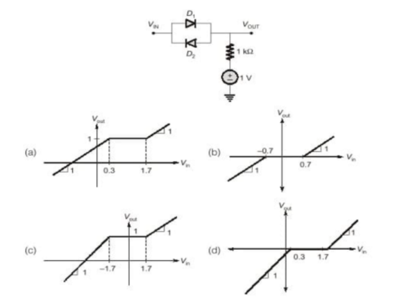
In the circuit shown below, D1 and D2 are silicon diodes with cut-in voltage 0.7 V. VIN and VOUT are input and output voltages in volts. The transfer characteristic is:
GATE 2023 Analog Electronics Q1 diode circuit diagram
Solution
Let \( V = 0.7\,V \):
Case I: Large positive \( V_{in} \) D1 ON, D2 OFF when \( V_{in} > 1 + 0.7 = 1.7\,V \). Then \( V_0 = V_{in} - 0.7 \).
Case II: Small \( V_{in} \) D1 OFF, D2 ON when \( 1 - V_{in} < 0.7 \) i.e. \( V_{in} < 0.3\,V \). Then \( V_0 = V_{in} + 0.7 \).
Case III: Middle range For \( 0.3 < V_{in} < 1.7\,V \), both diodes are OFF and the output is clamped by the 1-V source: \( V_0 = 1\,V \). The transfer characteristic has a flat segment at \( V_0 = 1 \) between \( V_{in} = 0.3 \) and \( 1.7 \) with linear slopes outside this range, matching Option A.
Question 02
Question 2
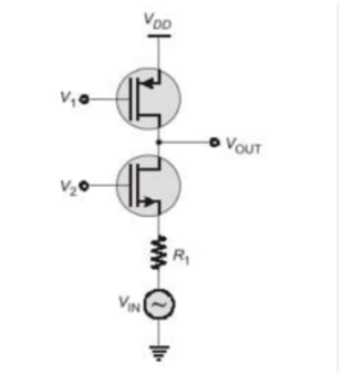
In the circuit shown below, V1 and V2 are bias voltages. Based on input and output impedances, the circuit behaves as a:
voltage controlled voltage source
voltage controlled current source
current controlled voltage source
current controlled current source
GATE 2023 Analog Electronics Q2 amplifier circuit diagram
Solution
From the circuit, M1 operates as a common-gate (CG) amplifier and M2 behaves as an active load. Using CG properties, \( R_{in} \) at the source is low, \( R_{out} \) is high. Thus, the stage is a current amplifier. A current amplifier corresponds to a current controlled current source (CCCS).
D
Final Answer
Correct option: D.
Question 03
Question 3
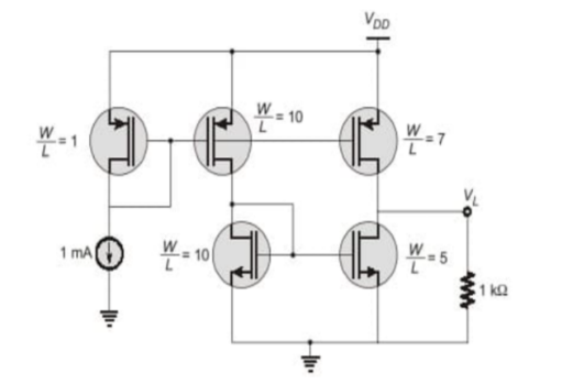
In the circuit below, the voltage \( V_L \) is ___ V, rounded off to two decimal places.
GATE 2023 Analog Electronics Q3 circuit diagram
Solution
Using \( I_D \propto W/L \) with the 1 mA reference branch: \( I_1 = 1\,mA,~ I_2 = 10 \times 1\,mA = 10\,mA \) \( I_3 = 10\,mA,~ I_4 = 7\,mA,~ I_5 = 5\,mA \) Output branch current \( I_0 = I_4 - I_5 = 7 - 5 = 2\,mA \) Across the 1 k\(\Omega\) load, \( V_L = I_0 \times 1 k = 2\,mA \times 1 k = 2.00\,V \).
Question 04
Question 4
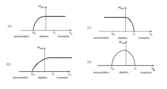
For a MOS capacitor, \( V_{fb} \) and \( V_t \) are the flatband and threshold voltages, respectively. The variation of depletion width \( W_{dep} \) with gate voltage \( V_g \) is best represented by
GATE 2023 Analog Electronics Q4 capacitor circuit diagram
Solution
We know for \( V_g < V_{fb} \), accumulation, no depletion charge, \( W_{dep} = 0 \). For \( V_{fb} < V_g < V_t \), depletion forms and increases with \( V_g \). For \( V_g > V_t \), strong inversion, \( W_{dep} \) becomes approximately constant. So the correct sketch is the one that starts at zero in accumulation, rises through depletion, and flattens after threshold, matching Option B.
Question 05
Question 5
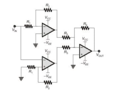
The gain \( \frac{V_{out}}{V_{in}} \) of the circuit shown below is
\( \frac{R_4}{R_3} \)
\( -\frac{R_4}{R_3} \)
\( 1 + \frac{R_4}{R_3} \)
\( 1 - \frac{R_4}{R_3} \)
GATE 2023 Analog Electronics Q5 op-amp circuit diagram
Solution
[Image of op-amp summer circuit analysis]
Identify the three op-amp stages: A1: Inverting amplifier, \( V_{01} = -\frac{R_2}{R_1} V_{in} \) A2: Non-inverting amplifier, \( V_{02} = (1 + \frac{R_2}{R_1}) V_{in} \) A3: Inverting summer with feedback/input ratio \( \frac{R_4}{R_3} \):
Equation
\[V_{out} = -\frac{R_4}{R_3} (V_{01} - V_{02}) \quad \text{(Assuming difference amplfier configuration based on result)}\]
Based on standard solution for this topology (assuming subtraction):