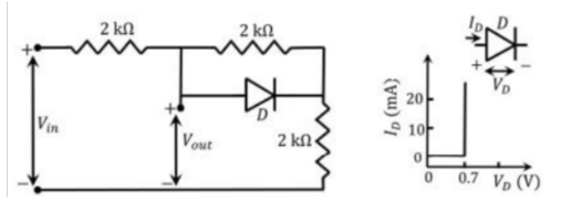
A circuit and the characteristics of the diode D in it are shown. The ratio of the minimum to the maximum small-signal voltage gain \(\frac{dV_{out}}{dV_{in}}\) is rounded off to two decimal places.
GATE 2022 Analog Electronics Q1 diode circuit diagram
Solution
Small-signal model: the source feeds \(V_{out}\) through one 2 k\(\Omega\) resistor, and from \(V_{out}\) a second 2 k\(\Omega\) resistor, shunted by the diode resistance \(r_d\), leads to the 2 k\(\Omega\) resistor that returns to ground.
Case I (diode ON, \(r_d = 0\)): the second 2 k\(\Omega\) is shorted out, so \(V_{out}\) sees 2 k\(\Omega\) to ground:
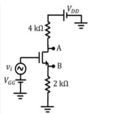
Consider the circuit shown with an ideal long-channel nMOSFET (enhancement mode, substrate tied to source). The transistor is biased in saturation with \(V_{GG}\) and \(V_{DD}\) so that it acts as a linear amplifier. \(v_i\) is the small-signal input. \(v_A\) and \(v_B\) are the small-signal node voltages at A and B, respectively. The value of \(v_A/v_B\) is rounded to one decimal place.
GATE 2022 Analog Electronics Q2 MOSFET circuit diagram
Solution
AC analysis: \(V_{DD}\) is a small-signal ground, so the small-signal drain current \(i_d\) flows down through the 4 k\(\Omega\) drain resistor and out through the 2 k\(\Omega\) source resistor. Node A is pulled below the AC ground while node B is pushed above it:
Consider an ideal long-channel nMOSFET (enhancement mode) with gate length \(L = 10\,\mu m\) and width \(W = 100\,\mu m\). The product \(\mu_n C_{ox} = 1\,mA/V^2\). The threshold voltage is \(V_T = 1\,V\). For \(V_{GS} = [2 - \sin(2t)]\,V\) and \(V_{DS}=1\,V\), substrate tied to source, the maximum value of the drain current is
40 mA
20 mA
15 mA
5 mA
Solution
\(V_{GS}\) peaks when \(\sin(2t) = -1\), giving \(V_{GS,max} = 3\,V\). Since \(V_{DS} = 1\,V < V_{GS,max} - V_T = 2\,V\), the device is in the triode (linear) region at the maximum current.
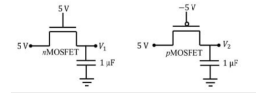
The ideal long-channel nMOSFET and pMOSFET devices in the circuits have threshold voltages of 1 V and -1 V, respectively. Substrates are tied to their sources. Ignore leakage, capacitors are initially discharged. For the applied supply voltages, the steady-state voltages are \(V_1\) and \(V_2\).
\(V_1=5\,V, V_2=5\,V\)
\(V_1=5\,V, V_2=4\,V\)
\(V_1=4\,V, V_2=5\,V\)
\(V_1=4\,V, V_2=5\,V\)
GATE 2022 Analog Electronics Q4 MOSFET circuit diagram
Solution
For the nMOS circuit (left) the gate is at 5 V and the capacitor node acts as the source. Charging stops when \(V_{GS}\) falls to \(V_T\), so \(5 - V_1 = 1\) and \(V_1 = 4\,V\): an nMOS passes a degraded logic high.
For the pMOS circuit (right) the gate is held at \(-5\,V\), so \(V_{SG} = V_2 + 5\) stays well above \(|V_T| = 1\,V\) all the way up. The device keeps conducting until the capacitor node equals the 5 V input, giving \(V_2 = 5\,V\): a pMOS passes an undegraded logic high.
C
Final Answer
Correct option: C.
Question 05
Question 5
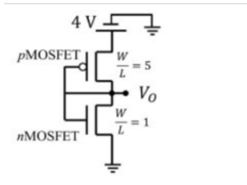
Consider the CMOS circuit shown (substrates tied to sources, gate \(W/L\) ratios as marked). Both devices have the same \(C_{ox}\) per unit area. For pMOS, \(V_T = -1\,V\), hole mobility \(= 40\). For nMOS, \(V_T = 1\,V\), electron mobility \(= 300\). The steady-state output voltage \(V_o\) is
equal to 0 V
more than 2 V
less than 2 V
equal to 2 V
GATE 2022 Analog Electronics Q5 NMOS circuit diagram
Solution
At DC, equate the magnitudes of the pMOS and nMOS currents in saturation:
Given \(\left(\frac{W}{L}\right)_p = 5\), \(\left(\frac{W}{L}\right)_n = 1\), \(\mu_p = 40\), \(\mu_n = 300\), \(V_{DD}=4\,V\), \(V_{Tp}=-1\,V\), \(V_{Tn}=1\,V\), with the gates tied to the output so that \(V_{in} = V_o\):
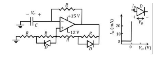
For the circuit shown (ideal op-amp), the difference between the maximum and minimum values of the capacitor voltage \(V_c\) is
15 V
27 V
13 V
14 V
GATE 2022 Analog Electronics Q6 op-amp circuit diagram
Solution
[Image of Astable multivibrator waveforms]
When op-amp output is at 15 V: divider at input gives \(V_{R}= 15 \times \frac{R}{3R} = 5\,V\), so \(V_{c,max}=5\,V\). When op-amp output is at -12 V: divider gives \(V_{R}= -12 \times \frac{2R}{3R} = -8\,V\), so \(V_{c,min}=-8\,V\). Required difference \(= 5 - (-8) = 13\,V\).
C
Final Answer
Correct option: C.
Question 07
Question 7
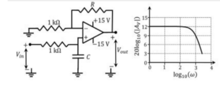
The following circuit uses an op-amp with supply voltages \(\pm 15\,V\), input \(V_{in}\), and feedback components \(R_1 = 10k\), \(R_2 = 90k\), and \(C=0.1\mu F\). Find the steady-state output voltage \(V_{out}\) when \(V_{in}=2\sin(2000t)\) V.
\(9\sin(2000t)\)
\(18\sin(2000t)\)
\(9\cos(2000t)\)
\(18\cos(2000t)\)
GATE 2022 Analog Electronics Q7 op-amp circuit diagram
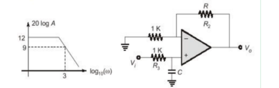
An ideal op-amp circuit with a sinusoidal input is shown. The 3 dB frequency is the frequency at which the magnitude of the voltage gain decreases by 3 dB from its maximum value. Which options are correct?
The circuit is a low pass filter.
The circuit is a high pass filter.
The 3 dB frequency is \(1000\,rad/s\).
The 3 dB frequency is \(1000\sqrt{3}\,rad/s\).
GATE 2022 Analog Electronics Q8 op-amp circuit diagram
Solution
[Image of low pass filter Bode plot]
The input reaches the non-inverting terminal through \(R_3\) with \(C\) to ground, and the op-amp itself is a non-inverting amplifier set by \(R_1\) and \(R_2\):
The magnitude is flat at low frequency and falls beyond \(\omega_c = \frac{1}{R_3C}\), so the circuit is a low pass filter. The given response is flat at 12 dB and is 3 dB down, at 9 dB, where \(\log_{10}\omega = 3\), so \(\omega_c = 1000\,rad/s\).