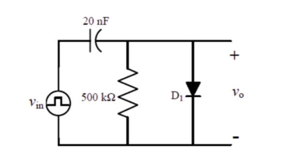
An asymmetrical periodic pulse train \( v_{in} \) of 10 V amplitude with on-time \( T_{ON} = 1\,ms \) and off-time \( T_{OFF} = 1\,s \) is applied to the circuit shown in the figure. The diode \( D1 \) is ideal. The difference between the maximum voltage and minimum voltage of the output waveform \( v_o \) in integer is V.
GATE 2021 Analog Electronics Q1 diode circuit diagram
Solution
In steady state, the capacitor charges to the peak input voltage when the diode is forward biased (ideal diode acts as a short).
Equation
\[V_C = V_{in,peak} = 10\,V\]
The output voltage is given by KVL:
Equation
\[V_{out} = V_{in} - V_C\]
During the ON time (\(T_{ON}\)), \(V_{in} = 10\,V\):
Equation
\[V_{out} = 10 - 10 = 0\,V\]
During the OFF time (\(T_{OFF}\)), \(V_{in} = 0\,V\) (assuming pulse goes 0 to 10V):
Equation
\[V_{out} = 0 - 10 = -10\,V\]
The difference between max and min output voltage:
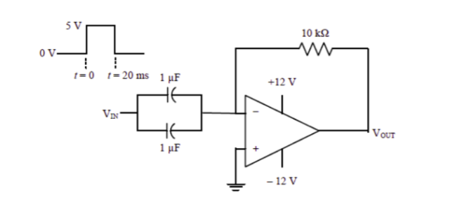
In the circuit shown below, a square wave of peak-to-peak amplitude 20 V and zero average value is applied. Assuming all components are ideal, what will be the average output voltage \( V_o \) across the resistor?
GATE 2021 Analog Electronics Q2 capacitor circuit diagram
Solution
A square wave with 20V peak-to-peak and zero average means it swings from -10V to +10V. The circuit configuration (series capacitor, shunt diode) is a clamper. - During the negative half cycle (\(V_{in} = -10V\)), the diode conducts and charges the capacitor to \(V_C = 10V\) (polarity: left plate -, right plate +). - The output voltage is \(V_{out} = V_{in} + V_C\). - When \(V_{in} = +10V\), \(V_{out} = 10 + 10 = 20V\). - When \(V_{in} = -10V\), \(V_{out} = -10 + 10 = 0V\). The output is a square wave swinging from 0V to 20V. The average value of this 0-20V square wave is:
Equation
\[V_{avg} = \frac{20 + 0}{2} = 10\,V\]
Thus, the average output voltage \( V_o = 10\,V \).
A
Final Answer
Correct option: A.
Question 03
Question 3
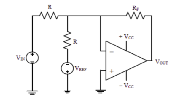
In the circuit shown below, assume ideal components. Determine the feedback factor \( \frac{V_f}{V_o} \) based on the configuration.
GATE 2021 Analog Electronics Q3 circuit diagram
Solution
MARKS TO ALL AS PER IIT ANSWER KEY. The feedback factor \(\beta = \frac{V_f}{V_o}\) is determined by the feedback network resistors. Based on the provided solution text (which seems disjointed, likely specific values were \(R_1, R_2, R_E\), etc.):