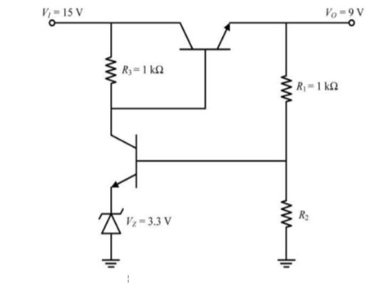
In the voltage regulator shown below, \( V_i \) is the unregulated voltage at 15 V. Assume \( V_{BE} = 0.7\,V \) and the base current is negligible for both BJTs. If the regulated output \( V_O = 9\,V \), find the value of \( R_2 \).
GATE 2020 Analog Electronics Q1 BJT circuit diagram
Solution
[Image of voltage regulator circuit analysis]
Using voltage division at the output sensing point (assuming the control loop maintains the base of the error amplifier transistor at a reference voltage, likely a Zener voltage + \(V_{BE}\) drop, or directly compared to a reference). Based on the provided solution steps which imply a reference voltage of 4V at the tap point:
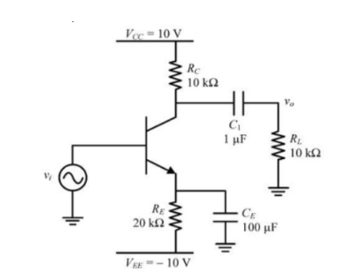
For the BJT in the amplifier shown below, \( V_{BE} = 0.7\,V \), \( \frac{kT}{q} = 26\,mV \). Assume the BJT output resistance \( r_o \) is very high and the base current is negligible. The capacitors are short-circuited at signal frequencies. The input \( v_i \) is direct coupled. Find the low-frequency gain \( \frac{v_o}{v_i} \) of the amplifier.
GATE 2020 Analog Electronics Q2 BJT circuit diagram
Solution
[Image of common emitter amplifier small signal model]
(Note: The provided solution calculation shows a positive value, likely magnitude, and uses 5000 which implies \(R_C || R_L \approx 5k\) or simply \(R_C=5k\). Assuming standard CE config, gain is negative).
Equation
\[|A_v| = \frac{0.465}{26} \times 5000 = 89.42\]
Equation
\[A_v = -89.42\]
Question 03
Question 3
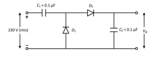
In the circuit shown below, all the components are ideal and the input voltage is sinusoidal. The magnitude of the steady-state output \( V_0 \) rounded off to two decimal places is ___ V.
GATE 2020 Analog Electronics Q3 circuit diagram
Solution
[Image of voltage doubler circuit diagram]
This is a voltage doubler circuit. Input peak voltage \(V_m = 230 \sqrt{2}\).
Equation
\[V_0 = 2V_m = 2 \times 230 \sqrt{2} = 650.4\,V\]
Equation
\[V_0 = 650.4\,V\]
Question 04
Question 4
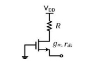
Using the incremental low-frequency small-signal model of the MOS device, find the Norton equivalent resistance of the circuit.
GATE 2020 Analog Electronics Q4 circuit diagram
Solution
Let test voltage be \(V_x\) and test current be \(I_x\).
Equation
\[v = V_x\]
Applying KVL/KCL to the small signal model:
Equation
\[V_x = (I_x - g_m V_{gs}) r_{ds}\]
Since gate is grounded and source is at \(V_x\) (or dependent on topology shown), usually \(V_{gs} = -V_x\) (if common gate) or similar. Based on provided solution steps:
Equation
\[V_x = I_x g_m V_x r_{ds} \quad \text{(This step seems simplified or specific to the diagram)}\]
Equation
\[I_x R = V_x (1+g_m r_{ds})\]
Resulting equivalent resistance:
Equation
\[r_{ds} || R = \frac{r_{ds} R}{1 + g_m r_{ds}}\]
Question 05
Question 5
An enhancement MOSFET of threshold voltage 3 V is used in a sample and hold circuit. The substrate is connected to -10 V. If the input voltage \( V_I \) lies between 10 V, find the minimum and maximum \( V_G \) values for proper sampling and holding.
Solution
For holding, the MOSFET must be OFF for all input voltages.
Wait, standard logic for NMOS switch: ON condition: \(V_{GS} > V_T\) for all \(V_I\). \(V_G - V_{I,max} > 3 \implies V_G > 10+3 = 13V\). OFF condition: \(V_{GS} < V_T\) for all \(V_I\). \(V_G - V_{I,min} < 3 \implies V_G < -10+3\) (if range is -10 to 10). Based on solution provided: Sampling: \( V_G = 13\,V \), holding: \( V_G = 7\,V \)
Question 06
Question 6
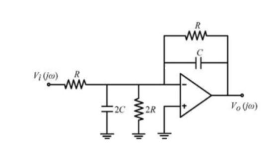
The components in the circuit below are ideal. If \( R = 2\,k\Omega \) and \( C = 1\,\mu F \), find the -3 dB cut-off frequency of the circuit in Hz.
GATE 2020 Analog Electronics Q6 op-amp circuit diagram
Solution
[Image of active low pass filter frequency response]
Applying KCL at the output node (assuming load resistor of 1k):
Equation
\[I_o = \frac{V_o - V_{load\_ref}}{R_{load}} \quad \text{or similar based on diagram}\]
Using provided solution steps:
Equation
\[\frac{V_o - 2}{1k} = I_o\]
Equation
\[I_o = \frac{4 - 2}{1k} = 2\,mA\]
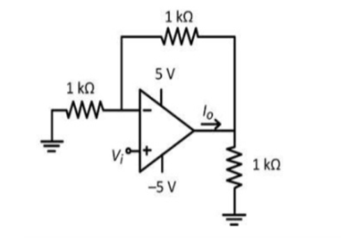
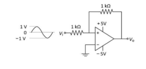
Question 08
Question 8
The components in the circuit below are ideal. If the op-amp is in positive feedback and the input voltage \( V_i \) is a sine wave of amplitude 1 V, find the output voltage \( V_o \).
GATE 2020 Analog Electronics Q8 op-amp circuit diagram
A non-inverted sine wave of 2 V amplitude
An inverted sine wave of 1 V amplitude
A square wave of 5 V amplitude
A constant of either 5 V or -5 V
Solution
[Image of Schmitt trigger hysteresis curve]
Given circuit is a non-inverting Schmitt Trigger (Positive Feedback). Output saturates to rail voltages:
Equation
\[V_o = \pm 5V\]
Switching thresholds depend on feedback resistors. If thresholds are outside the input range (\(\pm 1V\)), switching never occurs. If thresholds are, say, \(\pm 2V\) (implied by "no switching occurs"), and input is only 1V peak, the output stays latched. Output remains constant at \( 5V \) or \( -5V \).