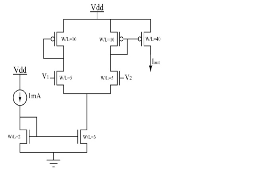
In the circuit shown, \(V_1 = 0\) and \(V_2 = V_{dd}\). The other relevant parameters are mentioned in the figure. Ignoring the effect of channel length modulation and the body effect, the value of \(I_{out}\) is \(\underline{\qquad}\) mA (rounded off to 1 decimal place).
GATE 2019 Analog Electronics Q1 circuit diagram
Solution
With \(V_1 = 0\) and \(V_2 = V_{dd}\) the left input device of the differential pair is off, so the whole tail current flows through the right one. The tail current is the \(1\,\textrm{mA}\) reference mirrored from the \(W/L = 2\) device into the \(W/L = 3\) device:
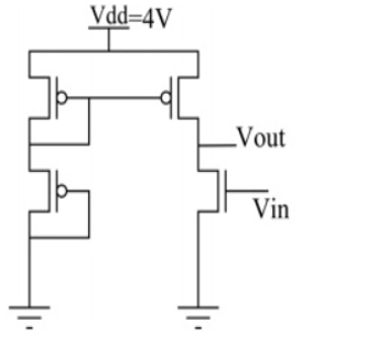
In the circuit shown, the threshold voltages of the pMOS (\(V_{tp}\)) and nMOS (\(V_{tn}\)) transistors are both equal to \(1\,V\). All transistors have the same output resistance \(r_{ds}\) of \(6\,\textrm{M}\Omega\). The other parameters are listed in the question. Ignoring the effect of channel length modulation and body bias, the gain of the circuit is \(\underline{\qquad}\) (rounded off to 1 decimal place).
GATE 2019 Analog Electronics Q2 NMOS circuit diagram
Solution
M3 and M4 are identical PMOS transistor and they have equal current. Hence, their \(V_{SG}\) should be equal. With \(V_{DD} = 4V\), \(V_{SG3} = V_{SG4} = 2V\). \( I_{SDP} = \mu_p C_{ox}\frac{W}{L}(V_{SG}-V_{tp})^2/2 = 30\,\mu A/V^2 \times 10 \times (2-1)^2 /2 = 150\,\mu A \) Current mirror gives \(I_{DSN} = I_{SDP} = 150\,\mu A\) M1 is a common source amplifier. \(A_v = -g_{m1}(r_{ds_2} \parallel r_{ds_1})\) \( g_{m1} = \sqrt{2 \mu_n C_{ox} \frac{W}{L} I_{DS}} \) using the values in the question. The equivalent load is \(3\,\textrm{M}\Omega\). Thus, \(A_v = -300 \times 3 = -900\).
✓
Final Answer
Correct answer: C.
Question 03
Question 3
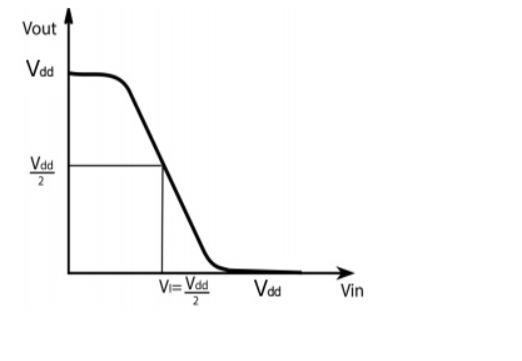
A CMOS inverter, designed to have midpoint voltage \(V_1\) equal to half of \(V_{dd}\), as shown, has: \( V_{dd}=3\,V,\; \mu_n C_{ox}=100\,\mu A/V^2,\; \mu_p C_{ox}=40\,\mu A/V^2,\\ V_{tn}=0.7\,V,\; |V_{tp}|=0.9\,V \) The ratio \(\left(\frac{W}{L}\right)_{nMOS}/\left(\frac{W}{L}\right)_{pMOS}\) equals \(\underline{\qquad}\) (rounded off to 3 decimals).
GATE 2019 Analog Electronics Q3 NMOS circuit diagram
Solution
At \(V_{in} = 1.5\,V\): Both nMOS and pMOS in saturation, currents equal. \(\displaystyle 100 \times (1.5-0.7)^2 = X \times 40 \times (1.5-0.9)^2\) \(\Rightarrow\) Ratio \(= \frac{40 \times 0.6^2}{100 \times 0.8^2} = 0.225\)
✓
Final Answer
Correct answer: B.
Question 04
Question 4
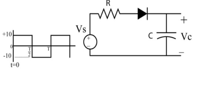
In the circuit shown, \(V_s\) is a \(10\,V\) square wave of period \(T=4\,ms\) with \(R=5 k\Omega\) and \(C=10\,\mu F\). The capacitor is initially uncharged at \(t=0\), and the diode is ideal. The voltage across the capacitor \((V_c)\) at \(3\,ms\) is \(\underline{\qquad}\) volts (rounded off to 1 decimal place).
GATE 2019 Analog Electronics Q4 diode circuit diagram
Solution
[Image of RC circuit charging discharging graph]
The time constant is \(\tau = RC = 5\times10^{3} \times 10\times10^{-6} = 50\,\textrm{ms}\). For \(0<t<2\)ms the source is \(+10\,\)V, the diode conducts and the capacitor charges from zero:
Equation
\[V_c(t) = 10\left(1 - e^{-t/\tau}\right)\]
At \(t=2\)ms this gives \(V_c = 10(1-e^{-0.04}) = 0.39\,\textrm{V}\). For \(2<t<4\)ms the source is \(-10\,\)V, the diode is reverse biased and the capacitor has no discharge path, so it holds that voltage:
Equation
\[V_c(3\,\textrm{ms}) = 0.4\,\textrm{V}\]
✓
Final Answer
\(V_c = 0.4\,\textrm{V}\).
Question 05
Question 5
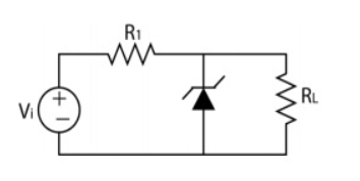
In the circuit shown, the breakdown voltage and maximum current of the Zener diode are \(20\,V\) and \(60\,mA\) respectively, \(R_1=200\,\Omega\), \(R_L=1k\Omega\). What is the range of \(V_i\) to ensure the Zener is 'on'?
GATE 2019 Analog Electronics Q5 Zener circuit diagram
22 V to 34 V
24 V to 36 V
18 V to 24 V
20 V to 28 V
Solution
With the Zener in breakdown the load current is fixed at \(I_L = V_Z/R_L = 20/1k = 20\,mA\). The series resistor carries \(I_{R_1}=I_L+I_Z\), so \(V_i = V_Z + I_{R_1}R_1\).
At the lower limit the Zener is just entering breakdown, \(I_Z = 0\), so \(I_{R_1} = 20\,mA\): \[V_{i,\min} = 20 + (20\,mA)(200\,\Omega) = 20 + 4 = 24\,V\]
At the upper limit the Zener carries its rated maximum, \(I_Z = 60\,mA\), so \(I_{R_1} = 80\,mA\): \[V_{i,\max} = 20 + (80\,mA)(200\,\Omega) = 20 + 16 = 36\,V\]
The Zener stays 'on' for \(24\,V < V_i < 36\,V\).
✓
Final Answer
Correct answer: B.
Question 06
Question 6
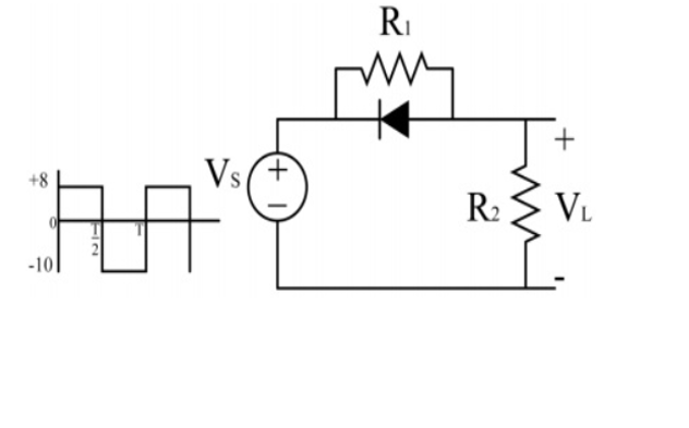
In the circuit shown, \(V_s\) is a square wave of period \(T\) with maximum and minimum values \(+8\,V\) and \(-10\,V\), respectively. Assume the diode is ideal and \(R_1 = R_2 = 500\,\Omega\). The average value of \(V_L\) is \(\underline{\qquad}\) volts (rounded off to 1 decimal place).
GATE 2019 Analog Electronics Q6 diode circuit diagram
Solution
When \(V_s=8\) V, diode is reverse-biased, so \(V_L=\frac{8 \times 500}{1000}=4V\). When \(V_s=-10\) V, diode is forward-biased, so \(V_L=-10\) V. Average over one period: \(\overline{V_L}=\frac{4 \times 0.5T+(-10) \times 0.5T}{T}=-3\) V.