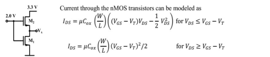
In the circuit shown below, the \((W/L)\) value for \(M_2\) is twice that for \(M_1\). The two nMOS transistors are otherwise identical. The threshold voltage \(V_T\) for both transistors is \(1.0\, V\). The voltage at \(V_2\) is (in volts, accurate to two decimal places):
GATE 2018 Analog Electronics Q1 MOSFET circuit diagram
Solution
[Image of MOSFET small signal model analysis]
Let \(K_n = \mu_n C_{ox} (W/L)\), \(K_2 = 2K_1\). For \(M_1\): \(V_{GS1} - V_T = 2-1 = 1\,V\), in linear region. For \(M_2\): \(V_{GS2} - V_T = 2-V_2-1 = 1-V_2\) and \(V_{DS2} = 3.3 - V_2 > (V_{GS2} - V_T)\) (saturation). Set \(I_{D1} = I_{D2}\):
Equation
\[K_1[2(1)V_1-V_1^2] = 2K_1(1-V_2)^2\]
Equation
\[2V_1-V_1^2 = 2(1+V^2_2-2V_2)\]
Solve: \(2V_1 - V_1^2 = 2(1 + V_2^2 - 2V_2)\), which simplifies to \(3V_2^2 - 6V_2 + 2 = 0\). Quadratic formula gives \(V_2 = 1.58\) or \(V_2 = 0.42\). Since \(V_{GS2} > V_T\), only \(V_2 = 0.42\) V is valid.
Question 02
Question 2
In the op-amp circuit shown, with ideal op-amp, what is the voltage (in volts, to one decimal place) at node A connected to negative input?
GATE 2018 Analog Electronics Q2 op-amp circuit diagram
Solution
The op-amp is in negative feedback, but the output rail is \(-15\)V (due to supply range). Applying KCL at node \(A\): \(\displaystyle \frac{V_A-(-15)}{31k} + \frac{V_A-1}{1k}=0 \implies 32V_A=16 \implies V_A = 0.5\,V\).
Question 03
Question 3
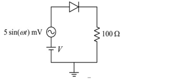
A DC current of \(26\,\mu\)A flows through the circuit shown. The diode (ideality 1) at quiescent point has junction capacitance \(0.5\) nF. Assume \(V_T=26\)mV. For \(\omega = 2\times10^6\) rad/s, small-signal input is \(5\sin(\omega t)\) mV across the diode. The amplitude of the small-signal component of diode current is (in \(\mu\)A, to one decimal place):
GATE 2018 Analog Electronics Q3 diode circuit diagram
A regulated \(5\)V is to be maintained across a \(1k\Omega\) resistor by the circuit. The Zener reverse breakdown starts from \(I_{zmin}=2\)mA, max allowed current \(I_{zmax}\); input \(V_1\) can vary by 5% from \(6\)V. Diode's breakdown resistance is negligible. The value of \(R\) and required minimum power dissipation of the diode are:
GATE 2018 Analog Electronics Q4 Zener circuit diagram
\(186\,\Omega\), \(10\,\)mW
\(100\,\Omega\), \(40\,\)mW
\(100\,\Omega\), \(10\,\)mW
\(186\,\Omega\), \(40\,\)mW
Solution
[Image of zener regulator circuit with variable input voltage]
\(V_1=6V\pm5\%=5.7\) to \(6.3\)V Load current \(I_L=5V/1k=5\)mA. Minimum current through resistor for zener to engage: \(I_s(min)=5+2=7\)mA. \(R=(V_1(min)-V_z)/I_s(min) = (5.7-5)/0.007 \approx 100\Omega\) \(R=100\Omega\): at \(V_1=6.3V\): \(I_s=13\)mA, so \(I_z(max)=13-5=8\)mA. So, \(P_{z}(min)=5V\times8\)mA = \(40\)mW. Correct answer: B
Question 05
Question 5
[2] A good transimpedance amplifier has:
Low input, high output impedance
High input, high output impedance
High input, low output impedance
Low input, low output impedance
Solution
[Image of transimpedance amplifier diagram]
Desirable: high input impedance (for current sensing), low output impedance (for load driving). Correct answer: C
Question 06
Question 6
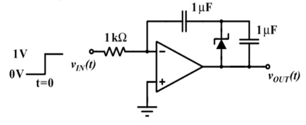
In the circuit shown below with ideal op-amp and unit step input \(v_{in}(t) = u(t)\), Zener voltage is \(2.5\)V, \(t=0\) capacitors are zero. At what time \(t\) (ms) does the output cross \(-10\)V?
GATE 2018 Analog Electronics Q6 op-amp circuit diagram
\(2.5\)
\(5.0\)
\(7.5\)
\(10.0\)
Solution
Input is step: \(v_{in}(t)=1\)V for \(t>0\). Current through \(1k\Omega\) is \(I=1mA\), charging \(C=1\mu\)F. \(V_{out}(t) = -\int I/C dt = -1V/\mu F \cdot t = -t\) mV per \(\mu\)s. \(V_{zener}=2.5V\) clamps deduced after \(t=2.5\)ms. To reach \(-10\)V: \(V_{out}= -10V \Rightarrow t=7.5\)ms. Correct answer: C
Question 07
Question 7
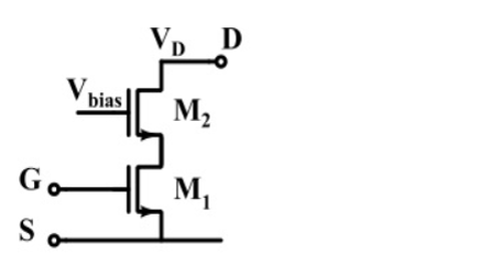
Two identical nMOS transistors \(M_1\) and \(M_2\) are connected as shown. Input between \(G\) and \(S\), output between \(D\) and \(S\). The transconductance \(g_m\) and output resistance \(r_o\) for the combination are best estimated as: