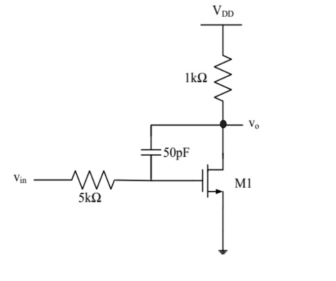
In the circuit shown below, transistor M1 is in saturation and has transconductance \(g_m = 0.01\) S. Ignoring internal parasitic capacitances and assuming channel length modulation \(\lambda = 0\), the small signal input pole frequency (in kHz) is:
GATE 2016 Analog Electronics Q1 transistor circuit diagram
Solution
The gain from input to output is calculated using Miller's equivalent circuit. Small-signal AC analysis yields the total resistance and capacitance at the input node.
[Image of Miller effect capacitance]
Pole frequency is \(f_p = \frac{1}{2\pi RC} = \frac{1}{2\pi \times 0.01 \times 50 \times 10^{-12}} = 57.87\,\text{kHz}\).
Question 02
Question 2
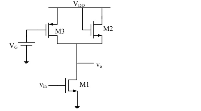
In the circuit shown below, channel length modulation of all transistors is non-zero, and all transistors operate in saturation with negligible body effect. The AC small signal voltage gain \(\frac{V_o}{V_{in}}\) of the circuit is:
GATE 2016 Analog Electronics Q2 transistor circuit diagram
\(g_{m1}r_{o1}r_{o3}\)
\(g_{m2}r_{o1}r_{o2}r_{o3}\)
\(g_{m1}r_{o1}r_{o3}r_{o2}\)
\(g_{m1}r_{o1}r_{o3}r_{o2}\)
Solution
[Image of Cascode amplifier small signal model]
With channel length modulation, output resistance per MOSFET is \(r_{o}\). For a cascode, the total gain is the product of \(g_m\) and all output resistances in the signal path. Therefore, \(A_v = g_{m1} r_{o1} r_{o3} r_{o2}\).
✓
Final Answer
Correct answer: C.
Question 03
Question 3
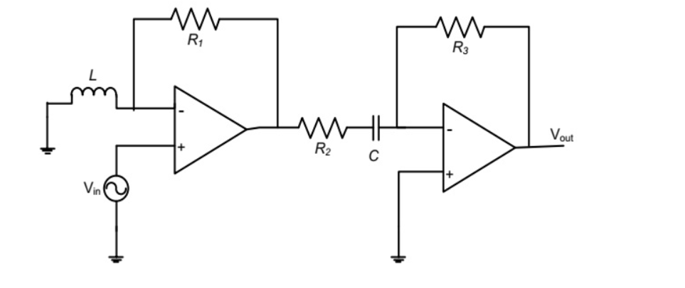
[2] For the circuit shown below, \(R_1 = R_2 = R_3 = 10~\Omega\), \(L = 1\) H and \(C = 1\) F. If the input \(V_{in} = \cos(10^6 t)\), then the overall voltage gain \(\frac{V_{out}}{V_{in}}\) is:
GATE 2016 Analog Electronics Q3 circuit diagram
Solution
[Image of RLC circuit resonance analysis]
Using phasor analysis, \(V_{out} = V_{in} \cdot (-1)\), due to the phase properties of the LC resonance with resistive load. Voltage gain is \(-1\).
Question 04
Question 4
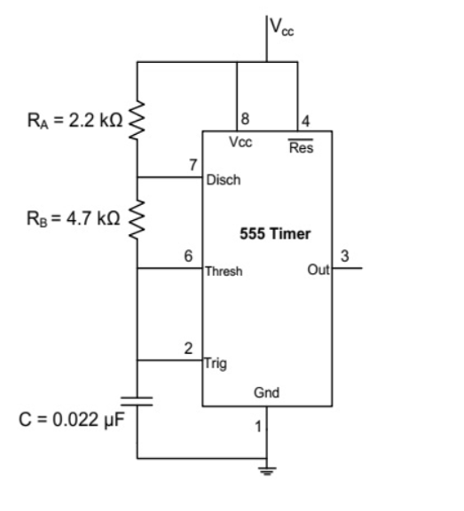
In the astable multivibrator circuit shown, the frequency of oscillation (in kHz) at output pin 3 is:
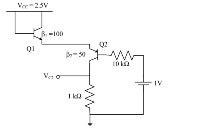
Consider the circuit shown below. Assuming \(V_{BE1} = V_{EB2} = 0.7\) V, the value of the DC voltage \(V_{C2}\) (in volts) is:
GATE 2016 Analog Electronics Q5 circuit diagram
Solution
Apply KVL: \(V_{C2} = V_{CC} - I_{C2} R_{C2}\); with \(V_{BE} = 0.7\) V. Solving gives \(V_{C2} = 0.5~\text{V}\).
Question 06
Question 6
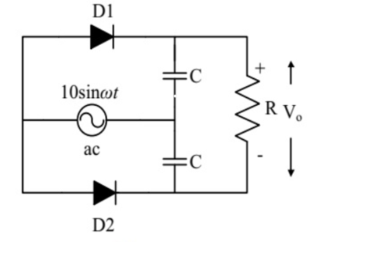
The diodes D1 and D2 in the figure are ideal and the capacitors are identical. The product RC is very large compared to the time period of the AC voltage. Assuming that the diodes do not breakdown in reverse bias, the output voltage \(V_o\) (in volt) at steady state is:
GATE 2016 Analog Electronics Q6 diode circuit diagram
Solution
Both diodes conduct during the first quarter positive cycle, then turn OFF. Both capacitors charge to peak input, output drops to zero afterward under steady state. So, \(V_o = 0~\)V.
Question 07
Question 7
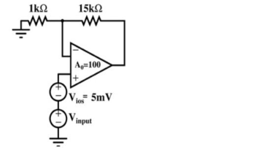
An opamp has a finite open loop voltage gain of 100. Its input offset voltage \(V_{ios}\) \(= 5\) mV is modeled as shown in the circuit below. The amplifier is ideal in all other respects. \(V_\text{input} = 25\) mV. The output voltage (in mV) is:
GATE 2016 Analog Electronics Q7 opamp circuit diagram
Solution
[Image of op amp input offset voltage model]
The actual differential input is \(V_\text{input} - V_{ios} = 20\) mV. Output is \(100\times20 = 2000\) mV. Closest value is \(2500\) mV.
✓
Final Answer
Correct answer: C.
Question 08
Question 8
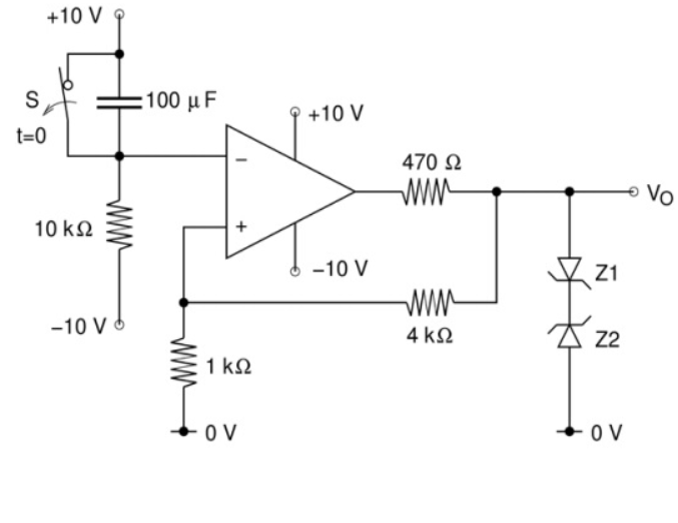
In the opamp circuit shown, the Zener diodes Z1 and Z2 clamp the output voltage V to 5 V or -5 V. The switch S is initially closed and is opened at time \(t_0\). The time \(t_T\) (in seconds) at which \(V_o\) changes state is:
GATE 2016 Analog Electronics Q8 opamp circuit diagram
Solution
Initially, Zener clamps at \(-5\) V. At \(t_0\), switch opens, capacitor charges exponentially. Apply the charging equation for capacitor; find time when voltage crosses \(+5\) V. Result: \(t_T = 0.798\) s.
Question 09
Question 9
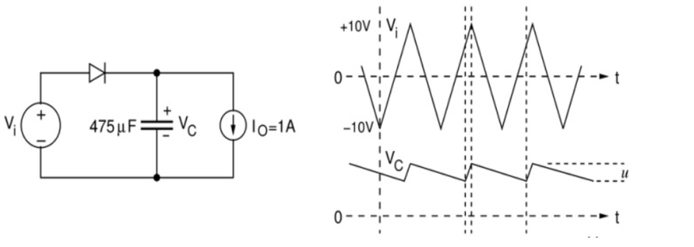
The figure shows a half-wave rectifier with a \(475\,\mu\)F filter capacitor. The load draws a constant current \(I=1\)A from the rectifier. The input voltage \(V_i\) is a triangle wave with an amplitude of \(10\) V, period of \(1\) ms. The value of the ripple \(u\) (in volts) is:
GATE 2016 Analog Electronics Q9 rectifier circuit diagram
Solution
Ripple voltage \(u = I/(fC)\) for half-wave; \(u = 1\times10^{-3}/(1 \times 475\times10^{-6}) = 2.15\) V.
✓
Final Answer
Correct answer: B.
Question 10
Question 10
Which one of the following statements is correct about an ac-coupled common-emitter amplifier operating in the mid-band region?
The device parasitic capacitances behave like open circuits, whereas coupling and bypass capacitances behave like short circuits.
The device parasitic capacitances, coupling capacitances and bypass capacitances behave like open circuits.
The device parasitic capacitances, coupling capacitances and bypass capacitances behave like short circuits.
The device parasitic capacitances behave like short circuits, whereas coupling and bypass capacitances behave like open circuits.
Solution
✓
Final Answer
Correct answer: A.
Question 11
Question 11
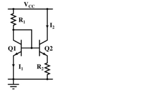
Resistor R in the circuit has been adjusted so that \(I=1\) mA. The bipolar transistors Q1 and Q2 are perfectly matched and have very high current gain. The supply voltage \(V_{cc}=6\) V. The thermal voltage \(kT/q=26\) mV. The value of \(R_2\) in \(\Omega\) for which \(I_2=100uA\) is:
GATE 2016 Analog Electronics Q11 transistor circuit diagram
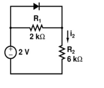
Assume the diode in the figure has \(V_{on} = 0.7\) V, but is otherwise ideal. The magnitude of current \(i_2\) (in mA) is:
GATE 2016 Analog Electronics Q12 diode circuit diagram
Solution
With diode ON, \(V_A = 2 - 0.7 = 1.3\) V across \(6~\Omega\): \(i_2 = 1.3/6 = 0.216~\)mA. Closest to \(0.25\) mA.
Question 13
Question 13
The Ebers-Moll model of a BJT is valid:
Only in active mode.
Only in active and saturation modes.
Only in active and cut-off modes.
In active, saturation and cut-off modes.
Solution
Model describes all three regions of operation: active, saturation, and cut-off—matching full transistor functionality.
✓
Final Answer
Correct answer: D.
Question 14
Question 14
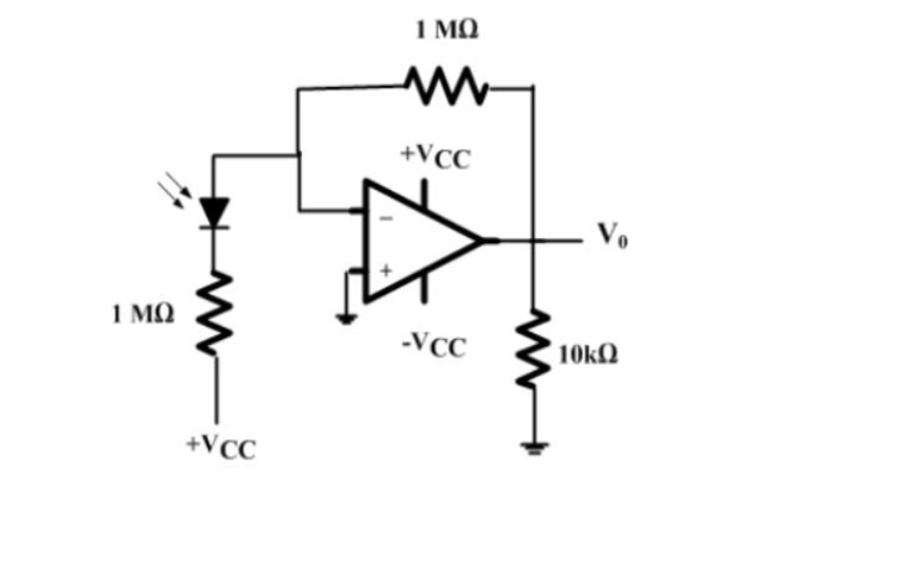
A p-i-n photodiode of responsivity \(0.8\) A/W is connected to the inverting input of an ideal opamp, \(V_{cc} = 15\) V, \(-V_{cc} = -15\) V, load resistor \(R = 10\) k\(\Omega\). \(10~\mu\)W power incident on photodiode. What is the photocurrent (in \(\mu\)A)?
GATE 2016 Analog Electronics Q14 opamp circuit diagram
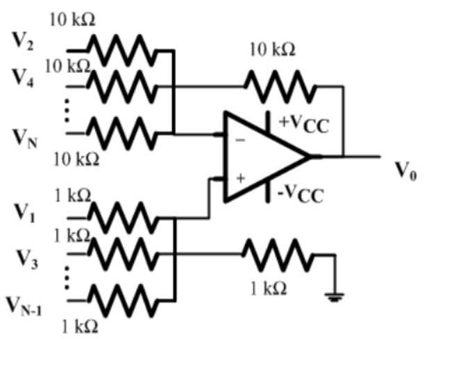
In the ideal opamp with voltages \(V_1, V_2, \ldots\), as \(N \rightarrow \infty\) and alternating+, what is the output voltage (in V)?
GATE 2016 Analog Electronics Q15 opamp circuit diagram
Solution
Large alternating sum forces opamp output to saturate to positive supply rail. Thus, output is \(15\) V.
✓
Final Answer
Correct answer: A.
Question 16
Question 16
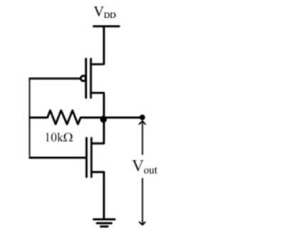
What is the voltage \(V_{out}\) in the following CMOS inverter circuit?
GATE 2016 Analog Electronics Q16 NMOS circuit diagram
\(A~V_{DD}\)
\(B~V_{TN}(\text{NMOS threshold})\)
\(C~\text{Switching threshold}\)
\(D~V_{TP}(\text{PMOS threshold})\)
Solution
[Image of CMOS inverter voltage transfer characteristics]
When input equals the switching threshold, NMOS and PMOS both conduct, \(V_{out}\) corresponds to inverter threshold.
✓
Final Answer
Correct answer: C.
Question 17
Question 17
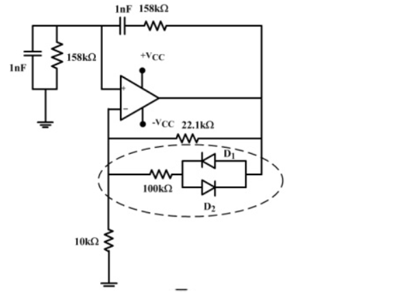
Consider the oscillator circuit shown. What is the function of the network (dotted box)?
GATE 2016 Analog Electronics Q17 opamp circuit diagram
Amplitude stabilization by preventing saturation of opamp (fixed sinusoidal oscillations).
Amplitude stabilization by forcing square wave oscillations.
Frequency stabilization at a single frequency.
Loop gain enables square wave oscillations.
Solution
Resistor-diode network limits output swing to below opamp rails, sustains sinusoidal oscillation with fixed amplitude.
✓
Final Answer
Correct answer: A.
Question 18
Question 18
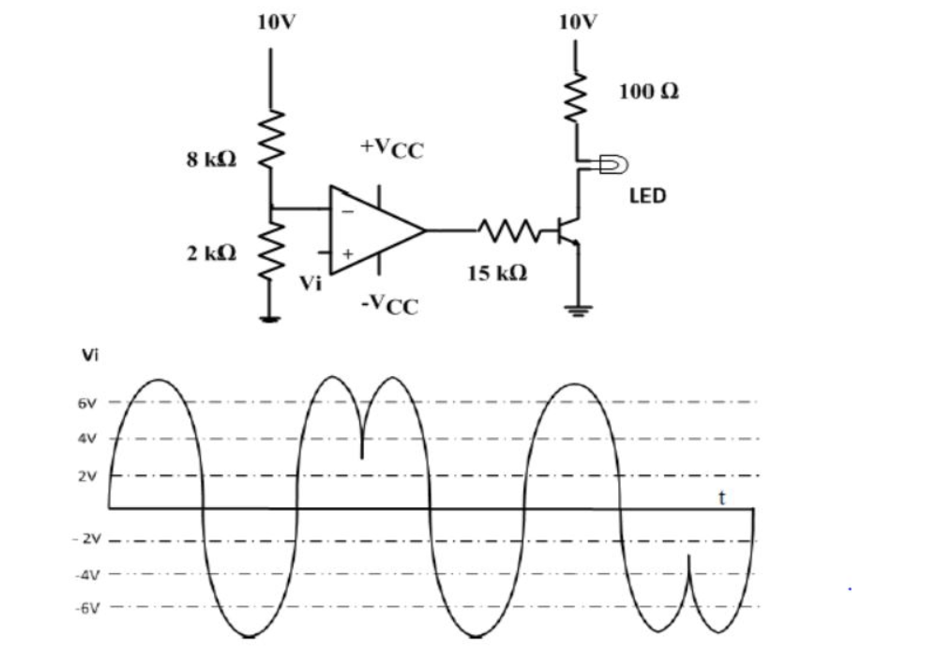
For the signal \(V_i\) (peak voltage \(8\) V) applied to non-inverting terminal of an opamp, transistor \(V_{BE}=0.7\)V, \(\beta =100\), \(V_{LED}=1.5\)V, \(V_{cc}=10\)V, \(-V_{cc}=-10\)V. How many times does the LED glow?
GATE 2016 Analog Electronics Q18 opamp circuit diagram
Solution
LED glows each time \(V_{i}>2\) V driving BJT/LED. Given waveform crosses above 2V threshold 3 times.