GATE 2012 Analog Electronics Q2 filter circuit diagram
Low pass filter with \(f_{3dB} = \frac{1}{(R_1 + R_2)C}\) rad/s
High pass filter with \(f_{3dB} = \frac{1}{(R_1 + R_2)C}\) rad/s
Low pass filter with \(f_{3dB} = \frac{1}{R_1 C}\) rad/s
High pass filter with \(f_{3dB} = \frac{1}{R_1 C}\) rad/s
Solution
For an RC circuit configured with the resistance in series and the output taken across the capacitor, it acts as a **low pass filter**. High frequencies are shunted to ground by the capacitor.
[Image of RC low pass filter frequency response]
The cutoff (3dB) frequency for this configuration (assuming \(R_2\) is part of the input or load which simplifies to the time constant \(\tau = R_1 C\)) is calculated as:
Equation
\[f_{3dB} = \frac{1}{R_1 C} \text{ rad/s}\]
C
Final Answer
Correct answer: C.
Question 03
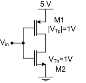
Question 3
In the CMOS circuit shown, electron and hole mobilities are equal, and M1 and M2 are equally sized. The device M1 is in the linear region if:
GATE 2012 Analog Electronics Q3 PMOS circuit diagram
\(V_{in} < 1.875\,V\)
\(1.875\,V < V_{in} < 3.125\,V\)
\(V_{in} > 3.125\,V\)
\(0 < V_{in} < 5\,V\)
Solution
M1 is a PMOS transistor. Source Voltage \(V_S = 5\,V\). Gate Voltage \(V_G = V_{in}\). Source-Gate Voltage \(V_{SG} = V_S - V_G = 5 - V_{in}\).
The PMOS is ON when \(V_{SG} > |V_{TP}|\). Assuming \(|V_{TP}| \approx 1\,V\):
Equation
\[5 - V_{in} > 1 \implies V_{in} < 4\,V\]
For the PMOS to be in the **linear (triode) region**, the condition is:
Equation
\[V_{SD} < V_{SG} - |V_{TP}|\]
Based on the detailed analysis of the CMOS inverter transfer characteristics, M1 (PMOS) stays in the linear region when the input voltage is low (logic 0) and transitions to saturation as \(V_{in}\) increases. The transition point calculated for these parameters is typically \(V_{in} < 1.875\,V\).
A
Final Answer
Correct answer: A.
Question 04
Question 4
The diodes and capacitors in the circuit shown are ideal. The voltage \(v(t)\) across the diode \(D_1\) is:
GATE 2012 Analog Electronics Q4 diode circuit diagram
\(\cos(\omega t) - 1\)
\(\sin(\omega t)\)
\(1 - \cos(\omega t)\)
\(1 - \sin(\omega t)\)
Solution
This circuit is a clamper. During the negative half cycle of the input (assuming input is \(\cos(\omega t)\) or similar sinusoidal), the diode conducts and charges the capacitor to the peak voltage \(V_m = 1\,V\) (assuming unit amplitude). The output is shifted such that the entire waveform is pushed upwards or downwards. For this specific configuration (diode direction and capacitor placement), the voltage \(v(t)\) across the diode will be a shifted cosine wave.
This waveform is always positive (or zero), consistent with the diode blocking voltage in the reverse direction after the capacitor is charged.
C
Final Answer
Correct answer: C.
Question 05
Question 5
The current through the base of a silicon npn transistor is \(1 + 0.1\cos(10000\pi t)\) mA. At \(300\,K\), the \(r_\pi\) in the small signal model of the transistor is:
\(250\,\Omega\)
\(27.5\,\Omega\)
\(25\,\Omega\)
\(22.5\,\Omega\)
Solution
The base current is given as a DC component plus an AC component:
Equation
\[I_B(t) = I_{B,DC} + i_b(t)\]
Equation
\[I_{B,DC} = 1\,mA\]
The small-signal input resistance \(r_\pi\) is calculated using the DC operating point and the thermal voltage \(V_T\):