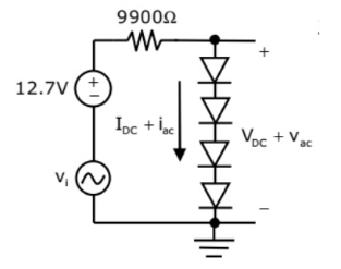
In the circuit shown below, assume that the voltage drop across a forward biased diode is \(0.7\,\mathrm{V}\). The thermal voltage \(V_t = KT/q = 25\,mV\). The small signal input \(v_i = V_p \cos(\omega t)\) where \(V_p = 100\,mV\).
GATE 2011 Analog Electronics Q1 diode circuit diagram
The ac output voltage \(V_{ac}\) is:
\(0.25\cos(\omega t) \text{ mV}\)
\(1\cos(\omega t) \text{ mV}\)
\(2\cos(\omega t) \text{ mV}\)
\(22\cos(\omega t) \text{ mV}\)
Solution
First, we perform a DC analysis to find the quiescent current \(I_{DC}\) to calculate the diode's dynamic resistance.
Since there are 4 diodes in series, the total dynamic resistance is \(r_{d,total} = 4 \times r_d = 100\,\Omega\). For the AC analysis, the circuit is a voltage divider. The AC output voltage \(V_{ac}\) is the voltage across the total dynamic resistance:
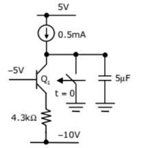
For the BJT \(Q_1\) in the circuit shown below, \(\beta = \infty\), \(V_{BEon} = 0.7\,\mathrm{V}\), \(V_{CEsat} = 0.7\,\mathrm{V}\). The switch is initially closed. At time t=0, the switch is opened. The time t at which \(Q_1\) leaves the active region is:
GATE 2011 Analog Electronics Q2 BJT circuit diagram
\(10\,ms\)
\(25\,ms\)
\(100\,ms\)
\(50\,ms\)
Solution
1. Find DC operating point (before t=0): The switch is closed, so \(V_C = 0\,\mathrm{V}\). We find the emitter current \(I_E\) by applying KVL to the base-emitter loop:
Since \(\beta = \infty\), \(I_C = I_E = 1\,mA\). The transistor is in the active region since \(V_{CE} = V_C - V_E = 0 - (-5.7) = 5.7\,\mathrm{V}\), which is \(> V_{CEsat}\).
2. Analyze for t > 0: At t=0, the switch opens. The base and emitter voltages are fixed, so \(I_C\) remains \(1\,mA\) (as long as it's active). The \(0.5\,mA\) current source and \(I_C\) both flow towards the collector node. The current \(I_{cap}\) that charges the capacitor is the difference (flowing away from the node):
3. Find saturation condition: The transistor leaves the active region and enters saturation when \(V_{CE} = V_{CEsat} = 0.7\,\mathrm{V}\). Since \(V_E\) is fixed at \(-5.7\,\mathrm{V}\), saturation occurs when:
4. Calculate time: The capacitor \(C = 5\,\mu F\) charges from \(V_C(0) = 0\,\mathrm{V}\) to \(V_{C(sat)} = -5.0\,\mathrm{V}\) with a constant current \(I_{cap} = 0.5\,mA\). Using the capacitor equation \(I = C \frac{dV}{dt}\), which for constant current is \(t = \frac{C \cdot |\Delta V|}{I}\):
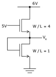
In the circuit shown below, for the MOS transistors, \(\mu_n C_{OX} = 100\,\mu A/V^2\) and the threshold voltage \(V_T = 1\,\mathrm{V}\). The voltage \(V_x\) at the source of the upper transistor is:
GATE 2011 Analog Electronics Q3 transistor circuit diagram
\(1\,\mathrm{V}\)
\(2\,\mathrm{V}\)
\(3\,\mathrm{V}\)
\(3.67\,\mathrm{V}\)
Solution
Both transistors are in series, so their drain currents are equal: \(I_{D1} = I_{D2}\). Let the upper transistor be M1 and the lower be M2.
Case 1 (+): \(8 - 2V_x = V_x - 1 \implies 9 = 3V_x \implies V_x = 3\,\mathrm{V}\). Case 2 (-): \(8 - 2V_x = -(V_x - 1) = -V_x + 1 \implies 7 = V_x\). We must check validity. If \(V_x = 7\,\mathrm{V}\), \(V_{GS1} = 5 - 7 = -2\,\mathrm{V}\), which is \(< V_T\), so M1 would be in cut-off. This solution is invalid. The correct solution is \(V_x = 3\,\mathrm{V}\).
C
Final Answer
Correct answer: C.
Question 04
Question 4
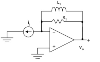
The circuit below implements a filter between the input current \(I_i\) and the output voltage \(V_o\). Assume that the opamp is ideal. The filter implemented is a:
GATE 2011 Analog Electronics Q4 opamp circuit diagram
low pass filter
band pass filter
band stop filter
high pass filter
Solution
This is a transimpedance (current-to-voltage) amplifier. The transfer function is \(H(s) = \frac{V_o(s)}{I_i(s)} = -Z_f\). The feedback impedance \(Z_f\) is the parallel combination of \(R_1\) and \(L_1\):
So, \(H(s) = - \frac{sR_1L_1}{R_1 + sL_1}\). We can analyze the filter's behavior at frequency extremes:
At \(\omega = 0\) (DC): \(s=0\). The inductor \(L_1\) acts as a short circuit (\(X_L = 0\)). This shorts the feedback path, making \(Z_f = 0\). Therefore, \(V_o = 0\). The gain is zero.
At \(\omega \to \infty\) (high frequency): \(s \to \infty\). The inductor \(L_1\) acts as an open circuit (\(X_L \to \infty\)). The feedback path is now just \(R_1\), so \(Z_f = R_1\). Therefore, \(V_o = -I_i \cdot R_1\). The gain is a constant \(-R_1\).
The filter has zero gain at low frequencies and a constant, non-zero gain at high frequencies, so it is a high pass filter.
D
Final Answer
Correct answer: D.
Question 05
Question 5
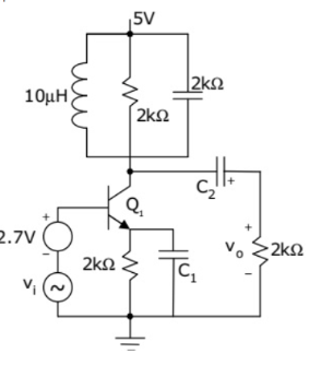
In the circuit shown below, capacitors C1 and C2 are very large and are shorts at the input frequency. \(v_i\) is a small signal input. The gain magnitude \(|v_o/v_i|\) at \(10\,M rad/s\) is:
GATE 2011 Analog Electronics Q5 BJT circuit diagram
maximum
minimum
unity
zero
Solution
The collector load is a parallel \(RLC\) tank with \(L = 10\,\mu H\), \(C = 1\,nF\) and \(R_L = 2\,k\Omega\). The gain of the common-emitter stage is \(A_v = -g_m Z_{tank}\), so the gain follows the tank impedance. The tank resonates at
This is exactly the input frequency of \(10\,M rad/s\). At resonance the parallel tank presents its largest impedance, purely resistive, so the gain magnitude is maximum.