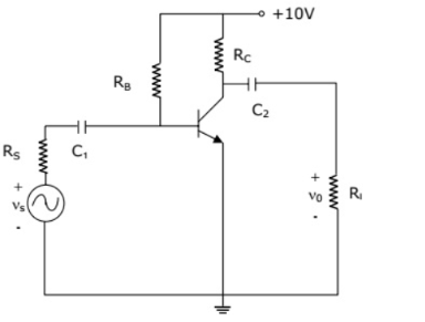
Consider the common emitter amplifier shown below with the following circuit parameters: \(\beta = 100\), \(g_m = 0.3861\,A/V\), \(r_0 = \infty\), \(r_a = \infty\), \(r_\pi = 259\,\Omega\), \(R_s = 1\,k\Omega\), \(R_B = 93\,k\Omega\), \(R_C = 250\,k\Omega\), \(R_L = 1\,k\Omega\), \(C_1 = \infty\) and \(C_2 = 4.7\,\mu F\).
GATE 2010 Analog Electronics Q1 amplifier circuit diagram
The lower cut-off frequency due to \(C_2\) is:
\(33.9\,Hz\)
\(27.1\,Hz\)
\(13.6\,Hz\)
\(16.9\,Hz\)
Solution
The lower cut-off frequency \(f_L\) due to the output coupling capacitor \(C_2\) is determined by \(C_2\) and the total resistance in its path. The resistance seen by \(C_2\) is the sum of \(R_C\) and \(R_L\).
Equation
\[f_L = \frac{1}{2\pi(R_C + R_L)C_2}\]
Note: The question text states \(R_C = 250\,k\Omega\), but the standard solution calculation uses \(R_C = 250\,\Omega\) to arrive at the correct answer options. This is likely a typo in the question text. Using \(R_C = 250\,\Omega\):
Consider the common emitter amplifier shown below with the following circuit parameters: \(\beta = 100\), \(g_m = 0.3861\,A/V\), \(r_0 = \infty\), \(r_a = \infty\), \(r_\pi = 259\,\Omega\), \(R_s = 1\,k\Omega\), \(R_B = 93\,k\Omega\), \(R_C = 250\,k\Omega\), \(R_L = 1\,k\Omega\), \(C_1 = \infty\) and \(C_2 = 4.7\,\mu F\).
GATE 2010 Analog Electronics Q2 amplifier circuit diagram
The resistance seen by the source \(v_s\) is:
\(258\,\Omega\)
\(1258\,\Omega\)
\(93\,\Omega\)
\(\infty\)
Solution
The resistance seen by the source \(v_s\) is \(R_{in}' = R_s + R_{in}\), where \(R_{in}\) is the input resistance of the amplifier stage. The input resistance \(R_{in}\) is the parallel combination of the biasing resistor \(R_B\) and the input resistance at the base of the transistor, \(h_{ie}\) (or \(r_\pi\)).
Equation
\[R_{in} = R_B || h_{ie}\]
The value of \(h_{ie}\) is given as \(r_\pi = 259\,\Omega\). We can also verify this:
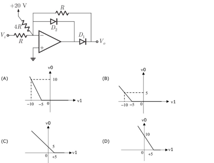
The transfer characteristic for the precision rectifier circuit shown below is (assume ideal OP-AMP and practical diodes):
GATE 2010 Analog Electronics Q3 op-amp circuit diagram
(Graph A)
(Graph B)
(Graph C)
(Graph D)
Solution
This is a summing amplifier circuit. Since the Op-Amp is ideal, \(V_+ = 0\,\mathrm{V}\), so \(V_- = 0\,\mathrm{V}\) (virtual ground). We can apply KCL at the \(V_-\) node (sum of currents entering = 0). This circuit acts as a precision half-wave rectifier and summing amplifier.
Case 1: \(V_o\) (at op-amp output, before D1) tends to go positive. This happens if \(\frac{V_i}{R} + \frac{20}{4R} > 0 \implies V_i + 5 > 0 \implies V_i > -5\,\mathrm{V}\). If \(V_{op-amp} > 0\), D1 is ON, D2 is OFF. The feedback loop is closed via D1, so \(V_o = V_- = 0\,\mathrm{V}\).
Case 2: \(V_o\) (at op-amp output) tends to go negative. This happens if \(V_i < -5\,\mathrm{V}\). If \(V_{op-amp} < 0\), D1 is OFF, D2 is ON. The feedback loop is now closed via D2 and \(R\). KCL at \(V_-\):
So, for \(V_i > -5\,\mathrm{V}\), \(V_o = 0\,\mathrm{V}\). For \(V_i \le -5\,\mathrm{V}\), \(V_o = -V_i - 5\). This matches graph (B).
B
Final Answer
Correct answer: B.
Question 04
Question 4
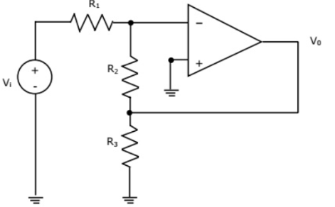
Assuming the OP-AMP to be ideal, the voltage gain of the amplifier shown below is:
GATE 2010 Analog Electronics Q4 op-amp circuit diagram
\(-\frac{R_2}{R_1}\)
\(-\frac{R_3}{R_1}\)
\(-\frac{R_2 || R_3}{R_1}\)
\(-(\frac{R_2+R_3}{R_1})\)
Solution
1. The non-inverting terminal \(V_+\) is connected directly to ground, so \(V_+ = 0\,\mathrm{V}\). 2. For an ideal Op-Amp in negative feedback, the virtual ground principle applies, so the inverting terminal \(V_-\) is also at \(0\,\mathrm{V}\). 3. Now consider resistor \(R_3\). One end is connected to \(V_-\) (which is at \(0\,\mathrm{V}\)) and the other end is connected to ground (\(0\,\mathrm{V}\)). 4. Since both ends of \(R_3\) are at the same potential, no current flows through it. \(R_3\) is effectively shorted out and has no impact on the circuit's operation. 5. The circuit simplifies to a standard inverting amplifier with \(R_1\) as the input resistor and \(R_2\) as the feedback resistor. 6. The voltage gain \(A_v\) for this configuration is:
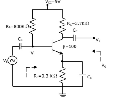
The amplifier circuit shown below uses a silicon transistor. The capacitors \(C_C\) and \(C_E\) can be assumed to be short at signal frequency and effect of output resistance \(r_0\) can be ignored. If \(C_E\) is disconnected from the circuit, which one of the following statements is true:
GATE 2010 Analog Electronics Q5 transistor circuit diagram
The input resistance \(R_i\) increases and magnitude of voltage gain \(A_v\) decreases.
The input resistance \(R_i\) decreases and magnitude of voltage gain \(A_v\) increases.
Both input resistance \(R_i\) and magnitude of voltage gain \(A_v\) decrease.
Both input resistance \(R_i\) and magnitude of voltage gain \(A_v\) increase.
Solution
When the emitter bypass capacitor \(C_E\) is connected, it provides a short to ground for AC signals, bypassing the emitter resistor \(R_E\). When \(C_E\) is disconnected, \(R_E\) is part of the AC circuit. This is known as emitter degeneration.
Input Impedance (\(R_i\)): With \(C_E\), the resistance seen from the base is just \(h_{ie}\) (or \(r_\pi\)). Without \(C_E\), the resistance seen from the base becomes \(R_{in(base)} = h_{ie} + (1+\beta)R_E\). This is a much larger value. The total input resistance \(R_i = R_B || R_{in(base)}\) will therefore increase.
Voltage Gain (\(A_v\)): With \(C_E\), the gain is high: \(|A_v| \approx \frac{R_C}{r_e}\). Without \(C_E\), the gain is significantly reduced due to negative feedback: \(|A_v| \approx \frac{R_C}{R_E}\). The magnitude of the voltage gain decreases.
Therefore, \(R_i\) increases and \(|A_v|\) decreases.
A
Final Answer
Correct answer: A.
Question 06
Question 6
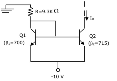
In the silicon BJT circuit shown below, assume that the emitter area of transistor \(Q_1\) is half that of transistor \(Q_2\). The value of current \(I_0\) is approximately:
GATE 2010 Analog Electronics Q6 BJT circuit diagram
\(0.5\,mA\)
\(2\,mA\)
\(9.3\,mA\)
\(15\,mA\)
Solution
This is a current mirror circuit. First, we find the reference current \(I_{REF}\) flowing through the \(R=9.3\,k\Omega\) resistor. The base of \(Q_1\) is \(V_B\). Since it's a silicon BJT, \(V_{BE} \approx 0.7\,\mathrm{V}\). The emitter is at \(-10\,\mathrm{V}\). Therefore, \(V_B = V_{BE} + V_E = 0.7\,\mathrm{V} + (-10\,\mathrm{V}) = -9.3\,\mathrm{V}\). This reference current \(I_{REF}\) flows from ground (\(0\,\mathrm{V}\)) to \(V_B\) through \(R\):
This current \(I_{REF}\) splits into \(I_{C1}\) and the base currents (\(I_{B1} + I_{B2}\)). Since \(\beta\) is very large (700+), we can neglect the base currents and assume \(I_{C1} \approx I_{REF} = 1\,mA\). For a current mirror, the collector current is proportional to the saturation current \(I_S\), which is proportional to the emitter area.