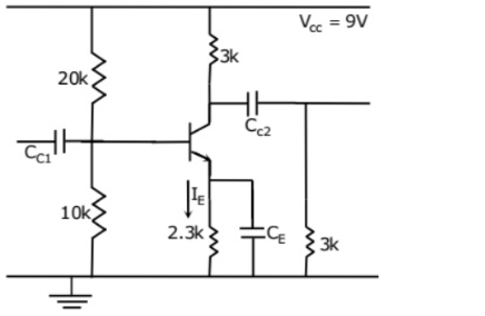
In the following transistor circuit \(V_{BE}=0.7\,\mathrm{V}\), \(r_e = 25\,mV/I_E\), and \(\beta\) and all the capacitances are very large. The mid-band voltage gain of the amplifier is approximately:
GATE 2008 Analog Electronics Q1 transistor circuit diagram
In the following transistor circuit \(V_{BE}=0.7\,\mathrm{V}\), \(r_e = 25\,mV/I_E\), and \(\beta\) and all the capacitances are very large. The value of DC current \(I_E\) is:
GATE 2008 Analog Electronics Q2 transistor circuit diagram
\(1\,mA\)
\(2\,mA\)
\(5\,mA\)
\(10\,mA\)
Solution
To find the DC current \(I_E\), we perform a DC analysis. The capacitors are open circuits. We find the Thevenin equivalent for the base-biasing network (\(20k\Omega\), \(10k\Omega\), and \(9V\)).
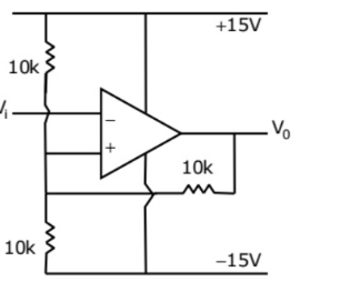
Consider the Schmidt trigger circuit shown below. A triangular wave which goes from \(-12\,\mathrm{V}\) to \(12\,\mathrm{V}\) is applied to the inverting input of OPAMP. Assume that the output of the OPAMP swings from \(+15\,\mathrm{V}\) to \(-15\,\mathrm{V}\). The voltage at the non-inverting input switches between:
GATE 2008 Analog Electronics Q3 opamp circuit diagram
\(-12\,\mathrm{V}\) to \(+12\,\mathrm{V}\)
\(-7.5\,\mathrm{V}\) to \(7.5\,\mathrm{V}\)
\(-5\,\mathrm{V}\) to \(+5\,\mathrm{V}\)
\(0\,\mathrm{V}\) and \(5\,\mathrm{V}\)
Solution
This is an inverting Schmitt trigger. The voltage at the non-inverting input (\(V_+\)) sets the trigger points. Based on the circuit configuration (assuming standard feedback resistors), the relationship is derived using KCL at the non-inverting node.
Equation
\[V_1 = \frac{V_0}{3}\]
Since \(V_0\) swings from \(-15\,\mathrm{V}\) to \(+15\,\mathrm{V}\):
Upper Trigger Point (\(V_{UTP}\)) occurs when \(V_0 = +15\,\mathrm{V}\):
The voltage at the non-inverting input switches between \(-5\,\mathrm{V}\) and \(+5\,\mathrm{V}\).
C
Final Answer
Correct answer: C.
Question 04
Question 4
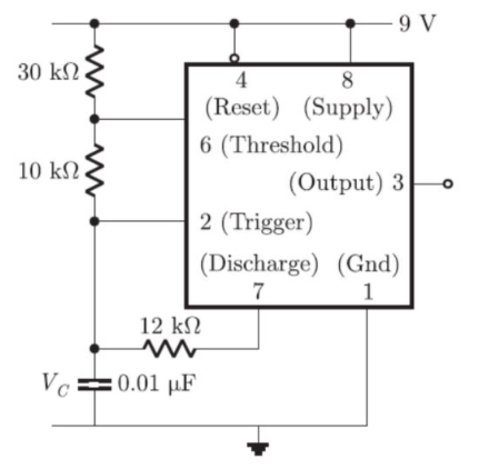
An astable multivibrator circuit using IC 555 timer is shown below. Assume that the circuit is oscillating steadily. The voltage \(V_C\) across the capacitor varies between:
GATE 2008 Analog Electronics Q4 capacitor circuit diagram
\(3\,\mathrm{V}\) to \(5\,\mathrm{V}\)
\(3\,\mathrm{V}\) to \(6\,\mathrm{V}\)
\(3.6\,\mathrm{V}\) to \(6\,\mathrm{V}\)
\(3.6\,\mathrm{V}\) to \(5\,\mathrm{V}\)
Solution
In a standard 555 timer astable configuration, the capacitor voltage \(V_C\) oscillates between the lower and upper threshold voltages. These internal thresholds are set by the 555's internal voltage divider:
The capacitor voltage \(V_C\) varies between \(3\,\mathrm{V}\) and \(6\,\mathrm{V}\).
B
Final Answer
Correct answer: B.
Question 05
Question 5
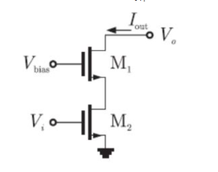
Two identical NMOS transistors M1 and M2 are connected as shown below. \(V_{bias}\) is chosen so that both transistors are in saturation. The equivalent \(g_m\) of the pair is defined to be \(\frac{\partial I_{out}}{\partial V_i}\) at constant \(V_{out}\). The equivalent \(g_m\) of the pair is:
GATE 2008 Analog Electronics Q5 NMOS circuit diagram
the sum of individual \(g_m\)'s of the transistors
the product of individual \(g_m\)'s of the transistors
nearly equal to the \(g_m\) of M1
nearly equal to \(g_m/g_0\) of M2
Solution
This configuration is a cascode stage (M1) on top of a common-source stage (M2). The input voltage \(V_i\) is the gate voltage of M2 (\(V_{GS2}\)).
Equation
\[I_{D2} = g_{m2} V_{GS2} = g_{m2} V_i\]
Since M1 is in series with M2, \(I_{out} = I_{D1} = I_{D2}\). The definition of the equivalent \(g_m\) is:
By definition, the transconductance of M2 is \(g_{m2} = \frac{\partial I_{D2}}{\partial V_{GS2}}\). Therefore, \(g_m = g_{m2}\). Since M1 and M2 are identical, \(g_{m1} = g_{m2}\). Thus, the equivalent \(g_m\) is nearly equal to the \(g_m\) of M1 (and M2).
C
Final Answer
Correct answer: C.
Question 06
Question 6
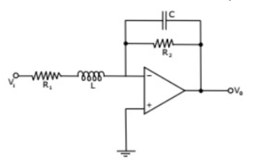
The OPAMP circuit shown above represents a:
GATE 2008 Analog Electronics Q6 opamp circuit diagram
high pass filter
low pass filter
band pass filter
band reject filter
Solution
This is an active inductor circuit. The transfer function \(H(s) = V_o/V_i\) is derived as:
Equation
\[H(s) = - \frac{Z_f}{Z_{in}}\]
Where \(Z_{in} = R_1 + Ls\) and \(Z_f = R_2 || \frac{1}{Cs}\).
This is a standard second-order low-pass filter transfer function, which has a constant numerator and a second-order polynomial in \(s\) in the denominator.
B
Final Answer
Correct answer: B.
Question 07
Question 7
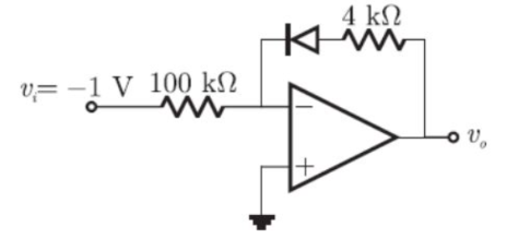
Consider the following circuit using an ideal OPAMP. The I-V characteristic of the diode is described by the relation \(I = I_0(e^{V/V_T} - 1)\) where \(V_T = 25\,mV\), \(I_0 = 1\,\mu A\) and V is the voltage across the diode (taken as positive for forward bias). For an input voltage \(V_i = -1\,\mathrm{V}\), the output voltage \(V_O\) is:
GATE 2008 Analog Electronics Q7 opamp circuit diagram
\(0\,\mathrm{V}\)
\(0.1\,\mathrm{V}\)
\(0.7\,\mathrm{V}\)
\(1.1\,\mathrm{V}\)
Solution
1. Since the op-amp is ideal, \(V_{-} = V_{+} = 0\,\mathrm{V}\). 2. The input current \(I_{in}\) is:
3. The feedback current \(I_f\) flows from \(V_o\) to \(V_{-}\). To balance the node, \(I_f = 10\,\mu A\). This current flows through the diode (forward biased). 4. Using the diode equation with \(I_D = I_f = 10\,\mu A\) and \(I_0 = 1\,\mu A\):
5. The output voltage \(V_o\) is the sum of the voltage drop across the \(4k\Omega\) resistor and the diode \(V_D\):
Equation
\[V_o = (I_f \times 4k\Omega) + V_D\]
Equation
\[V_o = (10\mu A \times 4000) + 0.06\]
Equation
\[V_o = 0.04 + 0.06 = 0.1\,\mathrm{V}\]
B
Final Answer
Correct answer: B.
Question 08
Question 8
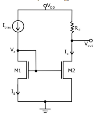
For the circuit shown in the following figure, transistor M1 and M2 are identical NMOS transistors. Assume the M2 is in saturation and the output is unloaded. The current \(I_x\) is related to \(I_{bias}\) as:
GATE 2008 Analog Electronics Q8 NMOS circuit diagram
\(I_x = I_{bias} + I_s\)
\(I_x = I_{bias}\)
\(I_x = I_{bias} - (V_{DD} - V_{out}) / R_E\)
\(I_x = I_{bias} - I_s\)
Solution
This is a standard NMOS current mirror circuit. The current \(I_{bias}\) flows into the drain of M1. M1 is "diode-connected" (\(V_{DS} = V_{GS}\)), ensuring it is in saturation. Since the gate of M2 is connected to the gate of M1, and their sources are both connected to ground, \(V_{GS2} = V_{GS1}\). Because M1 and M2 are identical transistors and have the same \(V_{GS}\), their drain currents must be equal:
Equation
\[I_{D1} = I_{D2}\]
Equation
\[I_{bias} = I_x\]
B
Final Answer
Correct answer: B.
Question 09
Question 9
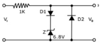
In the following limiter circuit, an input voltage \(V_i = 10\sin(100\pi t)\) is applied. Assume that the diode drop is \(0.7\,\mathrm{V}\) when it is forward biased. When it is forward biased, the zener breakdown voltage is \(6.8\,\mathrm{V}\). The maximum and minimum values of the output voltage respectively are:
GATE 2008 Analog Electronics Q9 Zener circuit diagram
\(6.1\,\mathrm{V}\), \(-0.7\,\mathrm{V}\)
\(0.7\,\mathrm{V}\), \(-7.5\,\mathrm{V}\)
\(7.5\,\mathrm{V}\), \(-0.7\,\mathrm{V}\)
\(7.5\,\mathrm{V}\), \(-7.5\,\mathrm{V}\)
Solution
This circuit clips (limits) the output voltage \(V_o\).
For the positive half of \(V_i\) (\(V_i > 0\)):
Diode D1 is forward biased.
Zener diode D2 is reverse biased.
The output clamps when D1 is on (\(0.7\,\mathrm{V}\) drop) AND D2 is in breakdown (\(6.8\,\mathrm{V}\) drop).