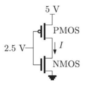
In the CMOS inverter circuit shown, if the trans conductance parameters of the NMOS and PMOS transistors are \(k_{n}=k_{p}=\mu_{n}C_{ox}\frac{W_{n}}{L_{n}}=\mu_{p}C_{ox}\frac{W_{p}}{L_{p}}=40\,\mu \mathrm{A} / \mathrm{V} ^2\) and their threshold voltages are \(V_{THn}=|V_{THp}|=1\,\mathrm{V}\) the current I is:
GATE 2007 Analog Electronics Q1 NMOS circuit diagram
\(0\,\mathrm{A}\)
\(25\,\mu \mathrm{A}\)
\(45\,\mu \mathrm{A}\)
\(90\,\mu \mathrm{A}\)
Solution
\(V_{GS}\) for each MOS is \(2.5\,\mathrm{V}\) \(V_{T}=1\,\mathrm{V}\), device parameter \(K=40\,\mu \mathrm{A} / \mathrm{V} ^2\) So, the drain current is:
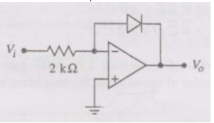
In the Op-Amp circuit shown, assume that the diode current follows the equation \(I=I_{s}exp(V/V_{T})\). For \(V_{i}=2\,\mathrm{V}\), \(V_{o}=V_{o1}\) and for \(V_{i}=4\,\mathrm{V}\), \(V_{o}=V_{o2}\). The relationship between \(V_{o1}\) and \(V_{o2}\) is:
GATE 2007 Analog Electronics Q2 op-amp circuit diagram
\(V_{o2}=\sqrt{2}V_{o1}\)
\(V_{o2}=e^{2}V_{o1}\)
\(V_{o2}=V_{o1}\ln 2\)
\(V_{o1}-V_{o2}=V_{T}\ln 2\)
Solution
For this log-amplifier circuit, the output voltage \(V_o\) is related to the input voltage \(V_i\) by:
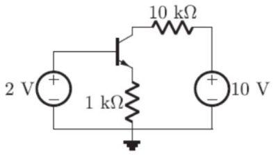
For the BJT circuit shown, assume that the \(\beta\) of the transistor is very large and \(V_{BE}=0.7\,\mathrm{V}.\) The mode of operation of the BJT is:
GATE 2007 Analog Electronics Q3 BJT circuit diagram
cut-off
saturation
normal active
reverse active
Solution
Given \(\beta\) is large, we can assume \(I_{B} \approx 0\) and \(I_{E} \approx I_{C}\). 1. Assume the BJT is in the active region. 2. Apply KVL in the Base-Emitter loop:
Since \(I_C \approx I_E\), \(I_{C(active)} = 1.3\,\mathrm{m} \mathrm{A}\). 3. Now, calculate the saturation current (\(I_{C(sat)}\)). This is the maximum possible current, assuming \(V_{CE(sat)} \approx 0.2\,\mathrm{V}\).
Since the calculated active region current (\(I_{C(active)}\)) is greater than the maximum possible saturation current (\(I_{C(sat)}\)), the transistor cannot be in the active region. It is driven into saturation.
B
Final Answer
Correct answer: B.
Question 04
Question 4
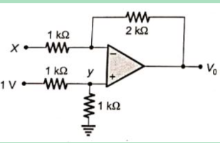
For the Op-Amp circuit shown in the figure, \(V_{0}\) is:
GATE 2007 Analog Electronics Q4 op-amp circuit diagram
\(-2\,\mathrm{V}\)
\(-1\,\mathrm{V}\)
\(-0.5\,\mathrm{V}\)
\(0.5\,\mathrm{V}\)
Solution
GATE 2007 Analog Electronics Q4 op-amp solution figure
Note: There appears to be a typo in the question's diagram. The inputs \(V_i=1.5\,\mathrm{V}\) and \(2\,\mathrm{V}\) lead to an answer (\(V_o=0\,\mathrm{V}\)) that is not in the options. The correct answer (C) is obtained if we assume the inputs were \(V_i=1\,\mathrm{V}\) and the other voltage source was \(1\,\mathrm{V}\).
Assuming \(V_i = 1\,\mathrm{V}\) and the other source is \(1\,\mathrm{V}\):
1. Find the voltage at the non-inverting terminal (\(V_+\)) using the voltage divider:
2. Due to the virtual short in an ideal Op-Amp, the inverting terminal voltage \(V_- = V_+ = 0.5\,\mathrm{V}\). 3. Now apply the superposition formula for a difference amplifier (or KCL at \(V_-\) node):
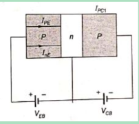
The common-base current gain \(\alpha\) is also the product of the emitter injection efficiency (\(\gamma\)) and the base transport factor (\(\beta^*\)):
Equation
\[\alpha = \gamma \times \beta^*\]
We are given \(\alpha \approx 0.98039\) and \(\gamma = 0.995\). We can solve for the base transport factor \(\beta^*\):
In a transconductance amplifier, it is desirable to have:
Solution
GATE 2007 Analog Electronics Q6 amplifier solution figure
A transconductance amplifier converts an input voltage (\(V_{in}\)) to an output current (\(I_{out}\)).
Input Resistance (\(R_{in}\)): The amplifier is sensing a voltage.
To sense the full voltage from a source without loading it (i.e., without drawing significant current), the input resistance should be as high as possible.
An ideal voltage-sensing input has infinite resistance (\(R_{in} \to \infty\)).
Output Resistance (\(R_{out}\)): The amplifier is delivering a current.
To deliver the full current to a load (and not have it shunted through its own output resistance), the output resistance should be as high as possible.
An ideal current source has infinite resistance (\(R_{out} \to \infty\)).
Therefore, it should have a large input resistance and a large output resistance.
A
Final Answer
Correct answer: A.
Question 07
Question 7
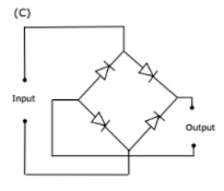
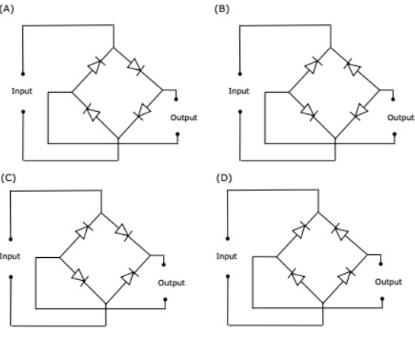
The correct full wave rectifier circuit is:
GATE 2007 Analog Electronics Q7 diode circuit diagram
Solution
Circuit (C) is a standard bridge rectifier.
During the positive half-cycle of the AC source, diodes D1 and D2 are forward-biased, and current flows through the load resistor.
During the negative half-cycle, diodes D3 and D4 are forward-biased, and current flows through the load resistor in the same direction.
Circuits (A), (B), and (D) are not configured correctly to achieve full-wave rectification.
C
Final Answer
Correct answer: C.
Question 08
Question 8
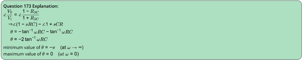
Consider the Op-Amp circuit shown in the figure. If \(V_{i}=V_{i1}\sin(\omega t)\) and \(V_{0}=V_{o1}\sin(\omega t + \phi)\), then the minimum and maximum values of \(\phi\) (in radians) are respectively:
GATE 2007 Analog Electronics Q8 op-amp circuit diagram
\(-\frac{\pi}{2}\) and \(\frac{\pi}{2}\)
\(0\) and \(\frac{\pi}{2}\)
\(-\pi\) and \(0\)
\(-\frac{\pi}{2}\) and \(0\)
Solution
GATE 2007 Analog Electronics Q8 op-amp solution figure
The transfer function \(H(s)\) for this circuit (which is a first-order all-pass filter) is:
The phase \(\phi\) ranges from \(-\pi\) to \(0\). The minimum value is \(-\pi\) and the maximum value is \(0\).
C
Final Answer
Correct answer: C.
Question 09
Question 9
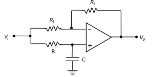
Consider the Op-Amp circuit shown in the figure. The transfer function \(V_{0}(s)/V_{i}(s)\) is:
GATE 2007 Analog Electronics Q9 op-amp circuit diagram
\(\frac{1-sRC}{1+sRC}\)
\(\frac{1+sRC}{1-sRC}\)
\(\frac{1}{1-sRC}\)
\(\frac{1}{1+sRC}\)
Solution
As derived in the previous question, the transfer function for this all-pass filter is found to be:
Equation
\[\frac{V_0(s)}{V_i(s)} = \frac{1-sRC}{1+sRC}\]
A
Final Answer
Correct answer: A.
Question 10
Question 10
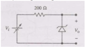
For the Zener diode shown in the figure, the Zener voltage at knee is 7V, the knee current is negligible and the Zener dynamic resistance is \(10\Omega\). If the input voltage (\(V_i\)) range is from 10 to 16 V, the output voltage (\(V_o\)) ranges from:
GATE 2007 Analog Electronics Q10 Zener circuit diagram
7.00 to 7.29 V
7.14 to 7.29 V
7.14 to 7.43 V
7.29 to 7.43 V
Solution
GATE 2007 Analog Electronics Q10 Zener solution figure
We model the Zener diode in its breakdown region as an ideal \(7\,\mathrm{V}\) DC source (\(V_Z\)) in series with its dynamic resistance (\(R_z = 10\,\Omega\)). The circuit can be analyzed using nodal analysis at the output node \(V_o\). The load is open, so no current flows to the right.