Analog Electronics: From Fundamentals to GATE Mastery
Analog electronics studies how continuous voltage and current signals are generated, amplified, shaped and conditioned using semiconductor devices. This complete revision guide walks through eleven core modules — beginning with semiconductor physics and ending with advanced building blocks such as data converters and switching regulators — followed by a quick-reference formula sheet and worked GATE-style examples. Throughout, the emphasis is on the relationships and formulas that recur most often in examinations.
Semiconductor Physics
Energy Band Theory
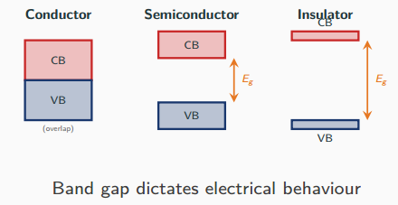
The electrical behaviour of a material is set by the gap between its valence and conduction bands. Conductors have overlapping valence and conduction bands; insulators have a large band gap \(E_g > 3\) eV; semiconductors have a small, intermediate gap.
- Silicon (Si): \(E_g = 1.12\) eV
- Germanium (Ge): \(E_g = 0.67\) eV
- Gallium Arsenide (GaAs): \(E_g = 1.43\) eV
Intrinsic and Extrinsic Semiconductors
- Intrinsic: pure material, \(n = p = n_i\), conductivity \(\sigma = q\,n_i(\mu_n + \mu_p)\).
- N-type (donor): Group V dopants (P, As, Sb); electrons are majority carriers; \(n \approx N_D\), \(p = n_i^2/N_D\).
- Group III dopants (B, Al, Ga).
- Holes are the majority carriers.
- \(p \approx N_A\), \(n = n_i^2/N_A\).
At 300 K, \(n_i\) for silicon \(\approx 1.5\times10^{10}\ \text{cm}^{-3}\). Memorise this — it appears in many GATE numericals.
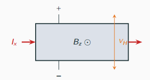
Hall Effect and the Continuity Equation
A magnetic field \(B_z\) applied to a current-carrying bar deflects carriers and produces a transverse Hall voltage \(V_H\). The sign of the Hall coefficient reveals the carrier type.
Diffusion lengths \(L_n, L_p\) govern BJT base transport and the diode reverse-saturation current \(I_S \propto 1/L_{n,p}\). These appear frequently in numerical problems.
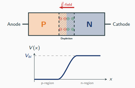
PN Junction and Diodes
Built-in Potential
I–V Characteristics and the Shockley Equation
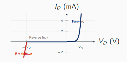
\(I_S\) is the reverse-saturation current; \(\eta\) the ideality factor (1 for Ge, 1–2 for Si); \(V_T = kT/q \approx 26\) mV at 300 K.
- Ideal: \(V_\gamma = 0\), \(r_d = 0\).
- Constant voltage drop: \(V_\gamma = 0.7\) V.
- Piecewise-linear: \(V_\gamma + r_d\).
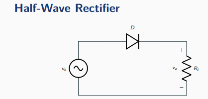
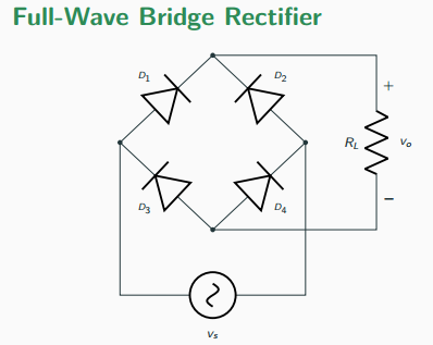
Rectifiers
Zener Diode and Voltage Regulation
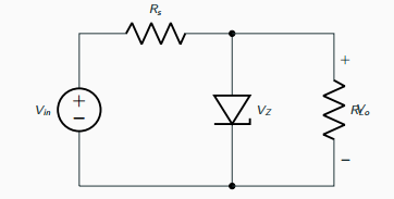
- Zener (heavy doping): \(V_Z < 5\) V, negative temperature coefficient.
- Avalanche (light doping): \(V_Z > 7\) V, positive temperature coefficient.
- Around 5–6 V both occur, giving near-zero TC.
Line regulation: \(\Delta V_o = \dfrac{r_Z}{R_s + r_Z}\,\Delta V_{in}\). Load regulation: \(\Delta V_o = -(r_Z \| R_s)\,\Delta I_L\), where \(r_Z\) is the Zener dynamic resistance.
Special Diodes
| Diode Type | Key Principle | Primary Application |
|---|---|---|
| Schottky | Metal–semiconductor junction; \(V_\gamma \approx 0.3\) V, no minority-carrier storage | High-speed switching, SMPS rectifiers |
| Zener | Reverse-breakdown regulation | Voltage references, regulators, clippers |
| Varactor | Voltage-variable capacitance, \(C_j \propto 1/\sqrt{V_R}\) | VCOs, tuned circuits, FM modulation |
| Tunnel | Quantum tunnelling; negative-resistance region | High-frequency oscillators and amplifiers |
| LED | Direct-bandgap recombination emits photons | Displays, indicators, optocouplers |
| Photodiode | Photons generate electron-hole pairs in the depletion region | Optical sensors, fibre-optic receivers |
| PIN | Intrinsic layer gives a wide depletion region | RF switches, high-voltage rectification |
Clippers and Clampers
- Removes the portion of a waveform above or below a reference level.
- Series or shunt configuration.
- Positive, negative or biased variants.
- Shifts the DC level without distorting the waveform shape.
- Uses a capacitor and diode, optionally with a bias.
- Positive or negative clamper.
For an ideal positive clamper the capacitor charges to \(V_m\) and holds it, so the output ranges from 0 to \(2V_m\). A negative clamper produces an output from \(-2V_m\) to 0.
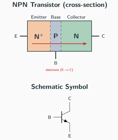
Bipolar Junction Transistor (BJT)
Structure and Basic Operation
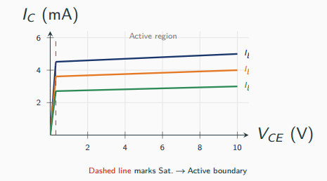
Operating Regions
| Region | EB Junction | CB Junction | Application |
|---|---|---|---|
| Cutoff | Reverse | Reverse | Switch OFF |
| Active | Forward | Reverse | Amplification |
| Saturation | Forward | Forward | Switch ON |
| Reverse Active | Reverse | Forward | Rarely used |
Biasing Techniques
| Biasing Scheme | Key Equation | Stability Factor \(S\) |
|---|---|---|
| Fixed bias | \(I_B = \dfrac{V_{CC}-V_{BE}}{R_B}\) | \(S = 1+\beta\) (poor) |
| Emitter bias | \(I_B = \dfrac{V_{CC}-V_{BE}}{R_B+(1+\beta)R_E}\) | \(S = \dfrac{1+\beta}{1+\beta R_E/(R_B+R_E)}\) |
| Collector-to-base | \(I_B = \dfrac{V_{CC}-V_{BE}}{R_B+(1+\beta)R_C}\) | \(S = \dfrac{1+\beta}{1+\beta R_C/(R_B+R_C)}\) |
| Voltage divider | \(V_{Th}=\dfrac{R_2 V_{CC}}{R_1+R_2},\ R_{Th}=R_1\|R_2\) | \(S = \dfrac{1+\beta}{1+\beta R_E/(R_{Th}+R_E)}\) (best) |
BJT Small-Signal Analysis
Hybrid-\(\pi\) Model
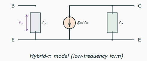
At \(I_C = 1\) mA, \(g_m = 38.5\) mA/V. With \(\beta = 100\), \(r_\pi \approx 2.6\ \text{k}\Omega\).
Amplifier Configurations
| Parameter | CE | CB | CC (Emitter Follower) |
|---|---|---|---|
| Voltage gain \(A_v\) | \(-g_m(R_C\|r_o)\) | \(+g_m(R_C\|r_o)\) | \(\approx 1\) |
| Current gain \(A_i\) | \(-\beta\) (high) | \(\alpha\;(\approx 1)\) | \(1+\beta\) (high) |
| Input resistance | \(r_\pi\) (medium) | \(r_e\) (low) | \(r_\pi + (1+\beta)R_E\) (high) |
| Output resistance | \(R_C\|r_o\) (high) | Very high | Very low \((\approx 1/g_m)\) |
| Phase shift | \(180^\circ\) | \(0^\circ\) | \(0^\circ\) |
| Application | Voltage amplifier | RF, buffer, cascode | Impedance matching |
- CE: high \(A_v\) and \(A_i\) — general purpose.
- CB: low \(R_{in}\), high bandwidth — RF amplifier.
- CC: high \(R_{in}\), low \(R_{out}\) — buffer.
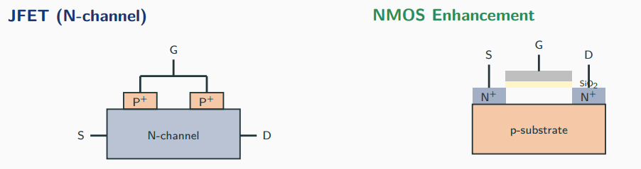
Field-Effect Transistors
JFET and MOSFET Structures
- Normally-ON (depletion-mode) device.
- \(V_{GS} \le 0\) (reverse bias on the PN gate).
- Pinch-off occurs at \(V_{GS} = V_P\).
- Normally-OFF (enhancement-mode) device.
- Requires \(V_{GS} > V_{Tn}\) to form a channel.
- Dominant device in modern integrated circuits.
FET: voltage-controlled, very high \(R_{in}\), unipolar, lower noise, no minority-carrier storage, smaller area. BJT: current-controlled, higher \(g_m\) per unit current, historically faster.
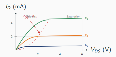
MOSFET I–V Characteristics
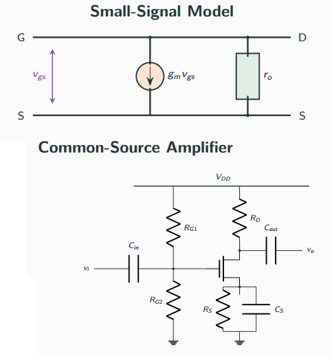
Small-Signal Model and CS Amplifier
MOSFET Configurations Summary
| Parameter | CS | CG | CD (Source Follower) |
|---|---|---|---|
| \(A_v\) | \(-g_m(R_D\|r_o)\) (high) | \(+g_m(R_D\|r_o)\) (high) | \(\dfrac{g_m R_S}{1+g_m R_S}\approx 1\) |
| \(R_{in}\) | \(R_{G1}\|R_{G2}\) (high) | \(1/g_m\) (low) | \(R_{G1}\|R_{G2}\) (high) |
| \(R_{out}\) | \(R_D\|r_o\) (high) | High | \(\approx 1/g_m\) (low) |
| Phase | \(180^\circ\) | \(0^\circ\) | \(0^\circ\) |
| Use | General amplifier | Cascode, RF | Buffer |
Cascode Amplifier: CS + CG Stack
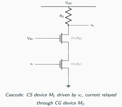
- \(M_1\) sees a low load (\(\approx 1/g_{m2}\)), so Miller multiplication of \(C_{gd1}\) is suppressed.
- Output resistance is boosted: \(R_{out}\approx g_{m2}\,r_{o2}\,r_{o1}\).
- DC gain \(|A_v|\approx g_{m1}(R_D \| R_{out})\).
- Bandwidth increases at constant gain.
When \(V_{SB}\neq 0\): \(V_{Tn} = V_{Tn0} + \gamma\!\left(\sqrt{2\phi_F + V_{SB}} - \sqrt{2\phi_F}\right)\), which adds a body transconductance \(g_{mb}\) in parallel with \(g_m\). The folded cascode restores headroom at low \(V_{DD}\) and is standard in CMOS op-amps.
Frequency Response
Amplifier Frequency Response
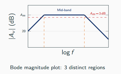
Sets \(f_L\): coupling capacitors \(C_{C1}, C_{C2}\) and the bypass capacitor \(C_E\) or \(C_S\). Sets \(f_H\): device capacitances \(C_\pi, C_\mu, C_{gs}, C_{gd}\); the Miller effect amplifies \(C_\mu\) / \(C_{gd}\).
Miller Effect and Gain-Bandwidth Product
- Input capacitance is multiplied by \((1+|A_v|)\).
- The dominant pole shifts to a lower frequency.
- Bandwidth is reduced.
- This is the primary motivation for the cascode topology.
Time-Constant Methods for \(f_L\) and \(f_H\)
Estimates the upper cutoff \(f_H\) from device capacitances:
- Set the input source to zero.
- Open all other capacitors; for each \(C_i\), find the resistance \(R_{io}\) seen by it.
- Sum the time constants: \(\tau_H = \sum_i R_{io}C_i\), so \(f_H \approx \dfrac{1}{2\pi\tau_H}\).
Estimates the lower cutoff \(f_L\) from coupling and bypass capacitors:
- Short every other capacitor; for each \(C_j\), find the resistance \(R_{js}\) seen by it.
- Sum the inverse time constants: \(\omega_L \approx \sum_j \dfrac{1}{R_{js}C_j}\), so \(f_L \approx \dfrac{\omega_L}{2\pi}\).
Feedback Amplifiers
Fundamental Concepts
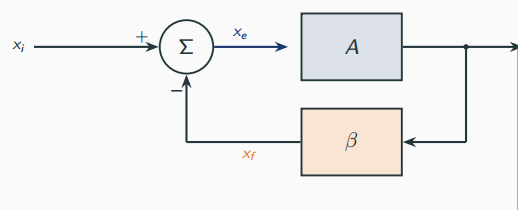
The signals are: input \(x_i\) and output \(x_o\); the error signal \(x_e = x_i - x_f\); and the feedback signal \(x_f = \beta x_o\).
Here \(A\beta\) is the loop gain and \(1 + A\beta\) the return difference. For \(A\beta > 0\) feedback is negative (\(|A_f|<|A|\)); for \(A\beta < 0\) it is positive (\(|A_f|>|A|\)); and \(A\beta = -1\) gives sustained oscillation.
Gain sensitivity is reduced by \((1+A\beta)\); distortion is divided by \((1+A\beta)\); bandwidth is multiplied by \((1+A\beta)\); and input/output impedances are modified in a topology-dependent way.
Four Feedback Topologies
| Topology | Sampled | Mixed | Stabilises |
|---|---|---|---|
| Voltage-Series (Series-Shunt) | Voltage | Voltage | Voltage gain \(A_v\) |
| Current-Series (Series-Series) | Current | Voltage | Transconductance \(G_m\) |
| Voltage-Shunt (Shunt-Shunt) | Voltage | Current | Transresistance \(R_m\) |
| Current-Shunt (Shunt-Series) | Current | Current | Current gain \(A_i\) |
- Series input ⇒ \(R_{in}\) increases.
- Shunt input ⇒ \(R_{in}\) decreases.
- Voltage output ⇒ \(R_{out}\) decreases.
- Current output ⇒ \(R_{out}\) increases.
In short: "make it look like what you sample."
Oscillators
Oscillator Fundamentals
For sustained sinusoidal oscillation two conditions must hold simultaneously:
- Magnitude: \(|A\beta| = 1\).
- Phase: \(\angle A\beta = 0^\circ\) (or \(360^\circ\)).
At start-up \(|A\beta|\gtrsim 1\); circuit nonlinearity then settles the loop gain to unity.
Crystal Oscillator
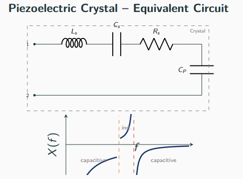
Quality factor \(Q \sim 10^4\)–\(10^6\), stability around 1 ppm, and an inductive reactance between \(f_s\) and \(f_p\) that oscillators exploit. Used in clocks, microcontrollers and communications.
Operational Amplifiers
Ideal versus Practical Op-Amp
- Open-loop gain \(A_{OL} = \infty\).
- Input resistance \(R_{in} = \infty\) (no input current).
- Output resistance \(R_{out} = 0\).
- \(BW = \infty\), CMRR \(= \infty\), slew rate \(= \infty\).
- Input offset voltage \(V_{OS}\) (mV).
- Input bias current \(I_B = (I_{B+}+I_{B-})/2\).
- Input offset current \(I_{OS} = |I_{B+}-I_{B-}|\).
- CMRR \(= 20\log(A_d/A_{CM})\) dB; PSRR for supply rejection.
- Slew rate \(SR = dV_o/dt|_{\max}\); finite GBW.
The Golden Rules
No current enters the inputs, and the output drives the input difference to zero (a virtual short). These two rules solve roughly 90% of GATE op-amp problems.
Op-Amp Circuit Zoo
| Circuit | Transfer Function | Notes |
|---|---|---|
| Summing amplifier | \(v_o = -R_f\!\left(\tfrac{v_1}{R_1} + \tfrac{v_2}{R_2} + \cdots\right)\) | Inverting; scales and sums inputs |
| Difference amplifier | \(v_o = \dfrac{R_f}{R_1}(v_2 - v_1)\) (matched) | CMRR depends on resistor matching |
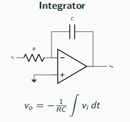
| Integrator | \(v_o = -\dfrac{1}{RC}\displaystyle\int v_i\,dt\) | Add \(R_f\) across \(C\) for DC stability |
| Differentiator | \(v_o = -RC\dfrac{dv_i}{dt}\) | Noise-sensitive; add input \(R_s\) |
| Instrumentation amp | \(A_v = \!\left(1+\tfrac{2R_1}{R_G}\right)\!\tfrac{R_3}{R_2}\) | Three-op-amp; very high CMRR |
| Voltage follower | \(v_o = v_i\) | \(A_v = 1\); highest buffer isolation |
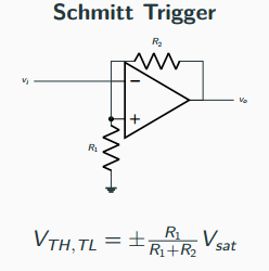
| Schmitt trigger (inv.) | \(V_{TH} = \dfrac{R_1}{R_1+R_2}V_{sat}\) | Hysteresis \(= V_{TH} - V_{TL}\) |
| Log amplifier | \(v_o = -V_T \ln(v_i / I_S R)\) | Diode or BJT in feedback |
| Active first-order LPF | \(A(s) = -\dfrac{R_f/R_1}{1 + sR_fC_f}\) | \(f_c = \dfrac{1}{2\pi R_f C_f}\) |
Integrator, Differentiator and Schmitt Trigger
Active Filters
| Filter Type | Transfer Function | Cutoff / Property |
|---|---|---|
| First-order LPF (inverting) | \(H(s) = -\dfrac{R_f/R_1}{1 + sR_fC}\) | \(f_c = \dfrac{1}{2\pi R_f C}\) |
| First-order HPF | \(H(s) = -\dfrac{sR_fC}{1 + sR_1C}\) | \(f_c = \dfrac{1}{2\pi R_1 C}\) |
| Sallen-Key LPF (2nd order) | \(H(s) = \dfrac{K\omega_o^2}{s^2 + (\omega_o/Q)s + \omega_o^2}\) | \(\omega_o = \dfrac{1}{\sqrt{R_1R_2C_1C_2}}\) |
| Butterworth | Maximally flat passband | \(Q = 1/\sqrt{2} = 0.707\) |
| Chebyshev | Equiripple passband | Sharper roll-off |
| Bessel | Linear phase | Best for pulse signals |
Power Amplifiers and Building Blocks
Power Amplifier Classes
| Class | Conduction | Max \(\eta\) | Distortion | Application |
|---|---|---|---|---|
| A | \(360^\circ\) | 25% (RC), 50% (xfmr) | Low | Audio (Hi-Fi) |
| B | \(180^\circ\) | 78.5% (\(\pi/4\)) | Crossover | Push-pull audio |
| AB | \(180^\circ\)–\(360^\circ\) | ~60–70% | Minimal | Most audio power stages |
| C | \(<180^\circ\) | 85–90% | Very high | RF (tuned load) |
| D | Switching (PWM) | >90% | Depends on PWM/filter | Modern audio, SMPS |
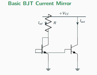
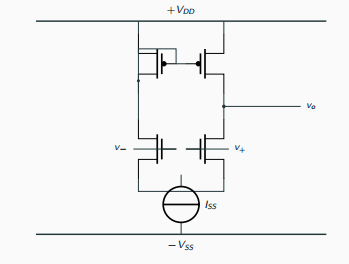
Differential Amplifier and Current Mirror
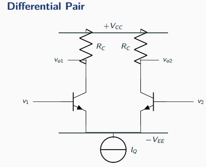
Differential Pair with Active Load
Advanced Current Mirrors
An emitter resistor \(R_E\) on the output transistor scales the current down: \(V_T \ln(I_{ref}/I_{out}) = I_{out}R_E\). It generates microamp bias currents without huge resistors.
Stacking a second mirror multiplies the output resistance: \(R_{out} \approx g_{m2}r_{o2}r_{o1}\). The penalty is an extra \(V_{BE}\) of headroom.
A three-transistor topology with feedback: \(I_{out} \approx I_{ref}(1 - 2/\beta^2)\), giving strong \(\beta\)-error compensation and \(R_{out}\approx \beta r_o/2\).
| Mirror | \(R_{out}\) | Headroom |
|---|---|---|
| Basic | \(r_o\) | 1 \(V_{BE}\) |
| Widlar | \(\sim r_o(1+g_m R_E)\) | 1 \(V_{BE}\) |
| Wilson | \(\beta r_o/2\) | 2 \(V_{BE}\) |
| Cascode | \(g_m r_o^2\) | 2 \(V_{BE}\) |
555 Timer and Voltage Regulators
- Series pass: transistor in series with the load; feedback adjusts \(V_o\) (78xx, LM317).
- Shunt: transistor in parallel with the load (less efficient).
- LDO: low-dropout regulator with a PMOS pass element.
Bandgap Reference and CMOS Transmission Gate
Sum two voltages with opposite temperature coefficients for a near-zero-TC reference: \(V_{BE}\) is CTAT (TC \(\approx -2\) mV/°C) and \(\Delta V_{BE} = V_T\ln(N)\) is PTAT. The result \(V_{ref} = V_{BE} + K V_T\ln(N) \approx 1.25\) V — the silicon bandgap extrapolated to 0 K. It anchors regulators (LM317, TL431) and ADC references.
An NMOS passes a clean logic 0 but loses \(V_{Tn}\) near the high rail; a PMOS does the opposite. Together they give a rail-to-rail pass with near-constant on-resistance. \(C=1\): both ON (closed switch); \(C=0\): both OFF (open switch). Used in sample-and-hold, multiplexers and ADC sampling.
Advanced Topics and GATE Extras
Capacitor Filter and Voltage Multipliers
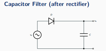
A half-wave doubler uses two diodes and two capacitors: \(C_1\) charges to \(V_m\), then \(C_2\) charges to \(2V_m\) via \(C_1\) and \(D_2\), giving \(V_{out} = 2V_m\) with PIV \(= 2V_m\). General \(N\)-stage output: \(V_o = N V_m\) (tripler, quadrupler, and so on).
Reverse Recovery and Second-Order BJT Effects
A positive-feedback loop \(T\uparrow \to I_C\uparrow \to P_D\uparrow \to T\uparrow\). Stability requires \(\partial P_C/\partial T_J < 1/\theta_{JA}\). Mitigations include emitter degeneration \(R_E\) and heat sinks; germanium is worse than silicon because of higher \(I_{CBO}\).
BJT h-Parameter Model
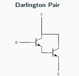
Darlington Pair and Multistage Coupling
| Coupling Type | Characteristics | Use |
|---|---|---|
| RC | Simple and cheap; DC blocked | Audio |
| Transformer | Impedance matching; bulky | RF, power |
| Direct | Passes DC; has drift | Op-amps, ICs |
| Tuned | Selective; narrow-band | RF stages |
Class AB Biasing and Power-Amp Refinements
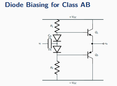
- Diodes bias both transistors slightly ON, eliminating crossover distortion.
- Each transistor conducts more than \(180^\circ\) but less than \(360^\circ\).
- A \(V_{BE}\)-multiplier gives adjustable bias; efficiency is roughly 60–70%.
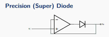
Precision Rectifier and Waveform Generators
V-to-I (grounded load): \(I_L = V_i/R_s\), independent of \(R_L\). I-to-V (transimpedance): \(V_o = -I_i R_f\), used with photodiodes. A sample-and-hold uses a buffer, a MOSFET switch and a hold capacitor: \(V_o(t)=V_i(t_s)\) with droop rate \(\Delta V/\Delta t = I_{leak}/C_H\).
Two-Stage Op-Amp Architecture
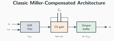
Stage 1 sets \(g_{m1}\) and the differential input; Stage 2 provides bulk gain; the buffer delivers low \(R_{out}\). The Miller capacitor \(C_c\) splits the poles, pushing \(f_{p1}\) down and \(f_{p2}\) up. The µA741 uses a 30 pF Miller capacitor giving a ~1 MHz GBW.
Stability, Phase Margin and Compensation
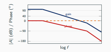
- Gain crossover \(f_{GX}\): \(|A\beta| = 1\) (0 dB).
- Phase crossover \(f_{PX}\): \(\angle A\beta = -180^\circ\).
- Phase Margin: \(\text{PM} = 180^\circ + \angle A\beta|_{f_{GX}}\).
- Gain Margin: \(\text{GM} = -20\log|A\beta|_{f_{PX}}\) dB.
- Dominant pole: add a large \(C_c\) to lower the first pole.
- Pole-zero: add an \(R_c\)–\(C_c\) network to insert a compensating zero.
- Miller (pole-splitting): place \(C_c\) across the high-gain stage to push \(f_{p1}\) down and \(f_{p2}\) up.
Noise in Amplifiers
Phase-Locked Loop (PLL)
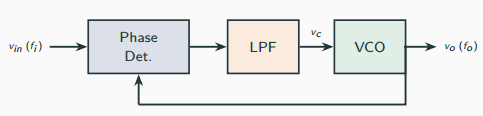
- Phase detector: compares the phases of \(f_i\) and \(f_o\).
- LPF: smooths the error into a DC control voltage.
- VCO: output frequency \(f_o \propto v_c\).
- Lock: \(f_o = f_i\) with a constant phase offset.
Lock range (kept-locked span), capture range (acquire-lock span, a subset of lock range), free-running frequency, and loop gain \(K_v = K_{PD}K_{VCO}\). Applications include FM demodulation, clock recovery, frequency synthesis, tone decoding and motor control.
Comparators, Log/Antilog and Analog Multipliers
Data Converters: ADC and DAC
- Weighted resistor: simple but needs \(R, 2R, \ldots, 2^{N-1}R\).
- R–2R ladder: only two resistor values; most popular.
- Current-steering: fastest, GHz update rates.
- \(\Sigma\)–\(\Delta\) DAC: oversampling plus noise shaping for Hi-Fi audio.
| ADC Type | Speed | Note |
|---|---|---|
| Flash | Fastest | \(2^N-1\) comparators |
| SAR | Medium | One comparator, \(N\) clocks |
| Pipeline | Fast | Multi-stage SAR |
| Dual-slope | Slow | Best noise rejection (DMM) |
| \(\Sigma\)–\(\Delta\) | Slow | 24-bit audio |
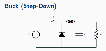
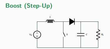
Switching Regulators (Buck and Boost)
CMOS Inverter and Special Devices
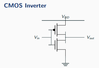
- \(V_{in}\) LOW: PMOS ON, NMOS OFF, so \(V_{out} = V_{DD}\).
- \(V_{in}\) HIGH: NMOS ON, PMOS OFF, so \(V_{out} = 0\).
- Near-zero static current; dynamic power \(P = C_L V_{DD}^2 f\).
- Switching point \(V_{in}\approx V_{DD}/2\) when matched.
UJT: a three-terminal negative-resistance device with intrinsic standoff ratio \(\eta = \tfrac{R_{B1}}{R_{B1}+R_{B2}}\) and peak voltage \(V_P = \eta V_{BB} + V_D\); used in relaxation oscillators and SCR triggering. SCR: a four-layer PNPN device that latches ON when gate-triggered and turns OFF only when \(I_A < I_H\); used in AC power control and motor drives.
GATE Formula Quick Reference
| Topic | Formula | Remarks |
|---|---|---|
| Thermal voltage | \(V_T = kT/q = 26\) mV @ 300 K | Constant — memorise |
| Diode current | \(I_D = I_S(e^{V_D/\eta V_T}-1)\) | \(\eta = 1\) (Ge), 1–2 (Si) |
| HWR | \(V_{dc} = V_m/\pi\), \(\eta = 40.6\%\) | \(\gamma = 1.21\) |
| FWR | \(V_{dc} = 2V_m/\pi\), \(\eta = 81.2\%\) | \(\gamma = 0.482\) |
| BJT currents | \(I_E = I_B + I_C\), \(\alpha = \beta/(1+\beta)\) | Fundamental |
| BJT \(g_m\) | \(g_m = I_C/V_T\) | Transconductance |
| BJT \(r_\pi\) | \(r_\pi = \beta/g_m = \beta V_T/I_C\) | Input resistance |
| CE gain | \(A_v = -g_m(R_C\|r_o)\) | Inverts signal |
| MOSFET sat. \(I_D\) | \(I_D = \tfrac{1}{2}\mu_n C_{ox}\tfrac{W}{L}V_{ov}^2\) | \(V_{ov} = V_{GS}-V_{Tn}\) |
| MOSFET \(g_m\) | \(g_m = \sqrt{2\mu_n C_{ox}(W/L)I_D} = 2I_D/V_{ov}\) | Three forms |
| Miller cap. | \(C_M = C(1 + |A_v|)\) | At input |
| Feedback | \(A_f = A/(1+A\beta)\) | Loop gain \(A\beta\) |
| Barkhausen | \(|A\beta| = 1\), \(\angle A\beta = 0^\circ\) | Oscillation condition |
| Wien bridge | \(f = 1/(2\pi RC)\), \(|A| \ge 3\) | RC oscillator |
| Colpitts | \(f = 1/(2\pi\sqrt{LC_{eq}})\), \(C_{eq} = C_1C_2/(C_1+C_2)\) | Two capacitors |
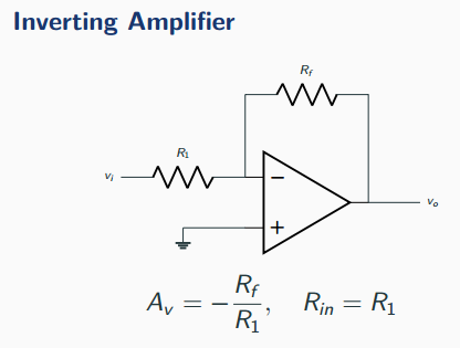
| Inverting op-amp | \(A_v = -R_f/R_1\) | Virtual ground |
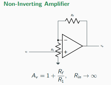
| Non-inverting op-amp | \(A_v = 1 + R_f/R_1\) | \(\ge 1\) |
| Slew rate | \(f_{\max} = SR/(2\pi V_p)\) | Full-power BW |
| Class B | \(\eta_{\max} = \pi/4 = 78.5\%\) | Push-pull |
| 555 astable | \(f = 1.44/((R_A+2R_B)C)\) | Duty \(> 50\%\) |
Common Pitfalls and Winning Strategies
- Confusing the \(\alpha\) and \(\beta\) formulas.
- Forgetting the Early effect in high-accuracy analysis.
- Ignoring the Miller effect at high frequencies.
- Wrong sign in the inverting op-amp gain.
- Mixing up HWR/FWR ripple factors.
- Using \(V_T = 26\) mV without checking the temperature.
- Overlooking the body effect in MOSFETs.
- Neglecting crossover distortion in Class B.
- Always draw the small-signal model.
- Use the virtual-ground concept for op-amp problems.
- Apply KCL at nodes and KVL around loops.
- Simplify with Thévenin/Norton at bias level.
- Verify units at every step.
- Estimate the order of magnitude before solving.
- For feedback, identify the topology, then \(A\) and \(\beta\).
Worked GATE-Style Examples
Example 1 — BJT Voltage-Divider Bias
Given \(V_{CC}=12\) V, \(R_1=47\) k\(\Omega\), \(R_2=10\) k\(\Omega\), \(R_C=3.3\) k\(\Omega\), \(R_E=1\) k\(\Omega\), \(\beta=100\) and \(V_{BE}=0.7\) V, find (a) \(I_{CQ}\) and \(V_{CEQ}\); (b) \(g_m\) and \(r_\pi\); (c) \(A_v\) with \(C_E\) across \(R_E\).
Step 1 — Thévenin at the base. \(V_{Th} = \tfrac{R_2}{R_1+R_2}V_{CC} = \tfrac{10}{57}(12) \approx 2.10\) V; \(R_{Th} = R_1\|R_2 \approx 8.25\) k\(\Omega\).
Step 2 — DC Q-point. \(I_B = \dfrac{V_{Th}-V_{BE}}{R_{Th}+(1+\beta)R_E} = \dfrac{1.40}{109.25\,\text{k}}\approx 12.8\ \mu\text{A}\); hence \(I_{CQ} = \beta I_B \approx 1.28\) mA and \(V_{CEQ} = V_{CC} - I_{CQ}(R_C+R_E) \approx 6.5\) V.
Step 3 — Small-signal parameters. \(g_m = I_{CQ}/V_T \approx 49.2\) mA/V; \(r_\pi = \beta/g_m \approx 2.03\) k\(\Omega\); \(r_e = V_T/I_{EQ} \approx 20\ \Omega\).
Step 4 — Voltage gain. With \(C_E\) shorting \(R_E\): \(A_v = -g_m R_C \approx -162\) V/V. Without \(C_E\) (full degeneration): \(A_v\approx -R_C/R_E = -3.3\) V/V — a 49× difference in swing.
Example 2 — Op-Amp Inverting Summer
An ideal op-amp has \(V_1 = +1\) V applied through \(R_1 = 10\) k\(\Omega\) and \(V_2 = +2\) V through \(R_2 = 20\) k\(\Omega\), both feeding the inverting input. The feedback resistor is \(R_f = 40\) k\(\Omega\) and \(v_+\) is grounded. Find \(V_o\).
Apply the golden rules (virtual ground \(v_- = 0\), \(I_- = 0\)) and KCL at the inverting node:
\[ \frac{V_1}{R_1} + \frac{V_2}{R_2} + \frac{V_o}{R_f} = 0 \] \[ V_o = -R_f\!\left(\frac{V_1}{R_1}+\frac{V_2}{R_2}\right) = -40\text{k}\!\left(\frac{1}{10\text{k}}+\frac{2}{20\text{k}}\right) = -8\ \text{V} \]Example 3 — Feedback Amplifier Sensitivity
A voltage-series feedback amplifier has \(A=10^4\) and \(\beta=0.01\). The open-loop gain \(A\) drops by 20% due to ageing. Find (a) \(A_f\) before and after, and (b) the percentage change in \(A_f\).
Using \(A_f = \dfrac{A}{1+A\beta}\): before, \(A\beta = 100\) so \(A_f^{(1)} = \dfrac{10^4}{101}\approx 99.01\). After a 20% drop, \(A' = 8000\), \(A'\beta = 80\), so \(A_f^{(2)} = \dfrac{8000}{81}\approx 98.77\). The change is \(\dfrac{\Delta A_f}{A_f}=\dfrac{99.01-98.77}{99.01}\approx 0.24\%\). A 20% drop in \(A\) produces only a 0.24% drop in \(A_f\).
Further Study and References
- Sedra & Smith, Microelectronic Circuits
- Boylestad & Nashelsky, Electronic Devices and Circuit Theory
- Millman & Halkias, Integrated Electronics
- Razavi, Fundamentals of Microelectronics
- Gray & Meyer, Analysis and Design of Analog ICs
- Previous-year GATE papers (solved)
- NPTEL lectures on analog electronics
- ACE / Made Easy practice books
- LTspice (free, by Analog Devices)
- NI Multisim
- Cadence Virtuoso (industry IC design)
- Proteus (beginner-friendly)
Mastering analog electronics is ultimately about recognising recurring building blocks — the biased transistor, the small-signal model, the feedback loop and the op-amp golden rules — and applying them consistently. As the closing thought of this course puts it: the best way to learn analog electronics is to build it.