Introduction to Thyristors
Definition
Thyristors are four-layer, three-terminal semiconductor devices, also known as Silicon Controlled Rectifiers (SCR)
Historical Context:
-
Invented by General Electric in 1957
-
Revolutionary impact on power electronics
-
Foundation of modern industrial control
Key Features:
-
High voltage capability (up to 12 kV)
-
High current handling (up to 6 kA)
-
Unidirectional current flow
-
Latching behavior - self-sustaining
Critical Property
Once triggered, thyristors cannot be turned off by gate control - requires current interruption
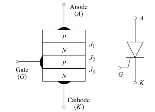
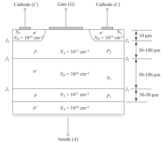
Thyristor Structure and Operation
Physical Structure:
-
Four alternating P-N layers (PNPN)
-
Three terminals: Anode, Cathode, Gate
-
Gate provides switching control
-
Junction areas determine ratings
Operating Principle:
-
Forward bias: \(V_{\mathrm{A}} > V_{\mathrm{K}}\)
-
Gate pulse initiates conduction
-
Internal regenerative feedback
-
Self-sustaining conduction
Key Insight
Three P-N junctions create unique switching behavior
Junction Behavior:
\(J_1\), \(J_3\) forward biased
\(J_2\) reverse biased (blocking)
Model Description:
-
\(T_1\) (PNP) and \(T_2\) (NPN) transistors
-
Regenerative feedback connection
-
Loop gain condition: \(\alpha_1 + \alpha_2 \geq 1\)
Current Analysis:
Critical Insight
When \(\alpha_1 + \alpha_2 \geq 1\), denominator → 0
Result: \(I_{\mathrm{A}} \to \infty\) (turn-on condition)
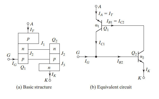
Operation Sequence:
-
Gate current increases \(\alpha_2\)
-
\(I_{\mathrm{C2}}\) becomes \(I_{\mathrm{B1}}\) for \(T_1\)
-
\(I_{\mathrm{C1}}\) feeds back to \(T_2\) base
-
Regenerative action sustains conduction
Self-reinforcing current amplification
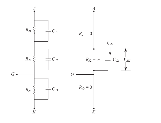
Transient Behavior and dv/dt Effects
Junction Modeling:
Any PN junction can be represented by a resistance (\(R_{\mathrm{J}}\)) and a capacitance (\(C_{\mathrm{J}}\)) in parallel.
-
Forward biased: \(R_{\mathrm{J}} = 0\), capacitance \(C_{\mathrm{J}}\) is negligible
-
Reverse biased: \(R_{\mathrm{J}} = \infty\), capacitance \(C_{\mathrm{J}}\) dominates
In SCR transient analysis:
-
Junctions \(J_1\) and \(J_3\) (forward biased): act as short circuits
-
Junction \(J_2\) (reverse biased): modeled by capacitance \(C_{J2}\)
Current through \(C_{J2}\):
Assuming \(C_{J2}\) is constant:
False Triggering
If \(\dfrac{\mathrm{d}V}{\mathrm{d}t}\) is high, \(I_{J2}\) increases. When \(I_{J2} > I_{\mathrm{L}}\) (latching current), SCR turns ON unintentionally.
Thyristor Characteristics
Forward Blocking State
-
Anode positive, no gate signal
-
Small leakage current (\(\mu\)A range)
-
Voltage limited by \(V_{\mathrm{BO}}\)
-
Junction \(J_2\) blocks current flow
Reverse Blocking State
-
Anode negative w.r.t. cathode
-
Small reverse leakage current
-
Blocks up to reverse rating
-
Junctions \(J_1\), \(J_3\) reverse biased
Forward Conducting State
-
Gate triggered OR voltage breakover
-
Low forward drop (\(\sim\) 1–2 V)
-
High current capability (kA range)
-
All junctions forward biased
Key Point: State depends on voltage polarity, current magnitude, and gate signal
VI Characteristics and Key Parameters
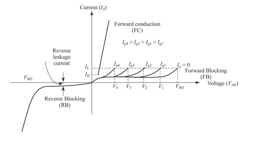
Design Implications:
-
Sharp switching transition
-
Hysteresis behavior
-
Gate control reduces \(V_{\mathrm{BO}}\)
Characteristic Regions:
-
Forward Blocking:
-
Low current until \(V_{\mathrm{BO}}\)
-
Controlled by gate current
-
-
Negative Resistance:
-
Unstable transition region
-
Rapid current increase
-
-
Forward Conduction:
-
High current, low voltage
-
Limited by external circuit
-
-
Reverse Blocking:
-
Small reverse current
-
Avalanche breakdown at \(V_{\mathrm{RBR}}\)
-
Critical Note
Gate loses control once thyristor turns ON
| Parameter | Description | Typical Range |
|---|---|---|
| \(V_{\mathrm{DRM}}\) | Peak repetitive forward blocking voltage | 400 V – 12 kV |
| \(V_{\mathrm{RRM}}\) | Peak repetitive reverse blocking voltage | 400 V – 12 kV |
| \(V_{\mathrm{DSM}}\) | Non-repetitive forward blocking voltage | \(1.1 \times V_{\mathrm{DRM}}\) |
| \(V_{\mathrm{RSM}}\) | Non-repetitive reverse blocking voltage | \(1.1 \times V_{\mathrm{RRM}}\) |
| \(V_{\mathrm{TM}}\) | Peak on-state voltage at rated current | 1.5 V – 3 V |
| \(V_{\mathrm{BO}}\) | Forward breakover voltage (no gate) | \(> V_{\mathrm{DRM}}\) |
Design Safety
Safety Factor: 2--3 times
Operating voltage \(\leq \frac{V_{\mathrm{DRM}}}{2.5}\)
Practical Note
Always include adequate derating for temperature and aging effects
Selection Criteria: Choose ratings 2–3\(\times\) operating values
| Parameter | Description | Typical Range |
|---|---|---|
| \(I_{T(\mathrm{RMS})}\) | RMS on-state current rating | 1 A – 6 kA |
| \(I_{T(\mathrm{AV})}\) | Average on-state current rating | \(0.6 \times I_{T(\mathrm{RMS})}\) |
| \(I_{\mathrm{TSM}}\) | Peak surge current (10 ms) | \(10 \times I_{T(\mathrm{AV})}\) |
| \(I_{\mathrm{H}}\) | Holding current (min to maintain ON) | 5 mA – 500 mA |
| \(I_{\mathrm{L}}\) | Latching current (min after gate removal) | 10 mA – 1 A |
| \(I_{\mathrm{GT}}\) | Gate trigger current | 0.5 mA – 200 mA |
Critical Relationship
Design Rule
Gate pulse width must ensure:
\(I_{\mathrm{anode}} > I_{\mathrm{L}}\) before gate removal
Temperature Effects: All currents decrease with increasing temperature
Thyristor Turn-ON Methods
| Method | Mechanism | Control | Application |
|---|---|---|---|
| Forward Voltage | \(V_{\mathrm{A}} > V_{\mathrm{BO}}\) | Poor | Not recommended |
| Gate Triggering | \(I_{\mathrm{G}} > I_{\mathrm{GT}}\) | Excellent | Most common |
| Temperature | High \(T_{\mathrm{j}}\) | None | Avoid (failure mode) |
| \(\dfrac{\mathrm{d}v}{\mathrm{d}t}\) | Fast voltage rise | None | False triggering |
| Light (LTT) | Photon energy | Good | Special applications |
Preferred Method: Gate Triggering
Advantages:
-
Precise timing control
-
Low power requirement
-
Reliable and repeatable
-
Fast response time
Typical Requirements:
-
Gate voltage: 1–3 V
-
Gate current: 10–200 mA
-
Pulse width: \(>\)1 \(\mu\)s
-
Rise time: \(<\)1 \(\mu\)s
Turn-ON Characteristics
Turn-ON Process Overview
Turn-ON Mechanism:
-
A thyristor turns ON when forward biased and a positive gate pulse is applied
-
Transition from forward OFF-state to ON-state takes finite time
-
Called turn-ON time (\(t_{\mathrm{on}}\))
Turn-ON time components:
-
Delay time (\(t_{\mathrm{d}}\))
-
Rise time (\(t_{\mathrm{r}}\))
-
Spread time (\(t_{\mathrm{p}}\))
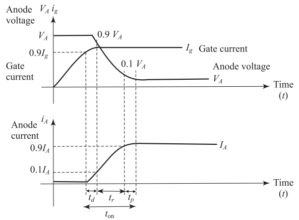
Detailed Turn-ON Time Analysis
Delay Time (\(t_{\mathrm{d}}\))
-
From gate trigger to 10% of final anode current
-
Anode-cathode voltage drops from \(0.9V_{\mathrm{d}}\) to \(0.1V_{\mathrm{d}}\)
-
Initial response phase
-
Typical: 0.1–1 \(\mu\)s
Key Point: Shortest phase of turn-on process
Rise Time (\(t_{\mathrm{r}}\))
-
Anode current rises from \(0.1I_{\mathrm{a}}\) to \(0.9I_{\mathrm{a}}\)
-
Anode voltage continues dropping
-
Strongly depends on gate drive current
-
Typical: 0.5–2 \(\mu\)s
Circuit Influence:
-
R-L circuits: Slower rise
-
R-C circuits: Faster rise
Spread Time (\(t_{\mathrm{p}}\))
-
Voltage drops to final ON-state value
-
Current reaches steady-state
-
Conduction spreads across cathode area
-
Longest: 1–3 \(\mu\)s
Physical Process: Current spreads laterally from gate region
Gate Triggering Design Guidelines
Essential Requirements:
-
Gate signal must be removed immediately after turn-ON
-
No gate signal when thyristor is reverse biased
-
Gate pulse width must ensure anode current reaches firing current
-
Gate current amplitude: 3 to 5 times the minimum triggering current
-
Higher gate current reduces turn-ON time
Design Equations:
where \(t_{\mathrm{safety}}\) accounts for circuit variations and temperature effects.
Temperature Considerations
Gate triggering requirements vary with temperature. Design for worst-case conditions.
Turn-OFF Characteristics
Turn-OFF Process Overview
Commutation Process:
-
A thyristor turns OFF when anode current falls below holding current (\(I_{\mathrm{H}}\))
-
This process is called commutation
-
Two methods: Natural commutation and Forced commutation
Turn-OFF time definition:
-
Time from anode current becoming zero until SCR regains forward blocking capability
-
Mathematically:
where \(t_{\mathrm{rr}}\) is reverse recovery time and \(t_{\mathrm{gr}}\) is gate recovery time\[\boxed{t_{\mathrm{off}} = t_{\mathrm{rr}} + t_{\mathrm{gr}}}\]
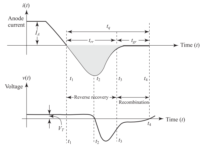
Reverse Recovery Time (\(t_{\mathrm{rr}}\))
Physical Process:
-
At \(t = t_1\): anode current becomes zero, initiating turn-OFF
-
Reverse recovery current flows due to stored charge carriers
-
During \(t_1\) to \(t_2\): charge carriers swept out from junctions \(J_1\) and \(J_2\)
-
At \(t_2\): 60% of stored carriers removed, reverse current magnitude reduces
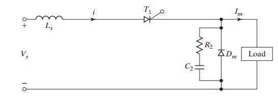
Design Considerations:
-
Rapid decay can induce reverse surge voltage
-
Mitigated using RC snubber circuits
-
Recovery charge relationship:
where \(Q_{\mathrm{rr}}\) is reverse recovery charge and \(I_{\mathrm{rr}}\) is peak reverse recovery current.
Typical Range
\(t_{\mathrm{rr}} = 5-30\,\mu\text{s}\) (depends on device construction and operating conditions)Gate Recovery Time (\(t_{\mathrm{gr}}\))
Final Recovery Phase:
-
At \(t_2\): reverse recovery current approaches zero
-
Thyristor can now block reverse voltage
-
However, junction \(J_3\) still contains stored charge carriers
-
Prevents effective forward voltage blocking capability
Recovery Process:
-
Reverse voltage must be applied to remove remaining carriers from \(J_3\)
-
Charge removal occurs through recombination processes (\(t_3\) to \(t_4\))
-
\(t_{\mathrm{gr}}\) represents time for complete charge recombination
-
At \(t_4\): thyristor fully turned OFF, can block forward voltage
Critical Design Point
Thyristor cannot reliably block forward voltage until \( t_{\mathrm{gr}} \) is completeTypical Range: 10–50 \(\mu\)s (varies with device type and temperature)
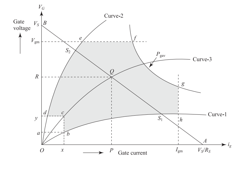
Gate Characteristics and Safe Operating Area
Gate Behavior:
-
SCR triggered by positive gate voltage (\(V_{\mathrm{g}}\)) or current (\(i_{\mathrm{g}}\))
-
Gate characteristics vary due to manufacturing tolerances
-
Gate-cathode junction behaves like a standard pn-junction diode
Critical Gate Parameters
-
\(i_{\mathrm{g,min}}\): Minimum gate current for reliable triggering
-
\(V_{\mathrm{g,min}}\): Minimum gate voltage for reliable triggering
-
\(V_{\mathrm{g,nt}}\): Non-triggering gate voltage (max safe level)
-
\(i_{\mathrm{g,max}}\), \(V_{\mathrm{g,max}}\): Maximum allowable gate parameters
-
\(P_{\mathrm{g,av}}\): Average gate power dissipation limit
Power Constraint:
Design Guidelines
-
Operate within shaded safe area of gate characteristics
-
Maintain noise immunity: signals below \(V_{\mathrm{g,nt}}\) threshold
-
Account for temperature variations and component tolerances
Gate Drive Circuit Analysis
Circuit Parameters:
-
\(V_{\mathrm{s}}\): Gate source voltage (DC supply)
-
\(R_{\mathrm{s}}\): Source resistance (current limiting)
-
\(V_{\mathrm{g}}\): Gate-cathode voltage drop
-
\(i_{\mathrm{g}}\): Gate current through circuit
Kirchhoff’s Voltage Law:
Load Line Equation:
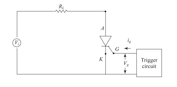
Load Line Analysis:
-
Load line intersects gate characteristic at operating point Q
-
Varying \(R_{\mathrm{s}}\) changes slope and operating point
-
Operating point should lie between min/max characteristics
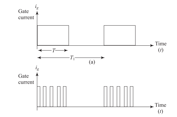
Pulse Triggering and Power Management
Pulse Triggering Advantages:
-
Increased gate current significantly reduces turn-ON time
-
Pulse width (\(T\)) must be \(\geq t_{\mathrm{on}}\) for reliable triggering
-
Allows higher instantaneous power for short durations
Power Relationships:
-
Maximum instantaneous gate power:
\[\boxed{P_{\mathrm{g,max}} = \frac{2 P_{\mathrm{g,av}}}{T}}\] -
Frequency-power relationship:
\[f = \frac{1}{T} \Rightarrow P_{\mathrm{g,av}} = \frac{P_{\mathrm{g,max}}}{2f}\]
Design Constraint
Always ensure \( V_{\mathrm{g}} \cdot I_{\mathrm{g}} < P_{\mathrm{g,max}} \) with adequate safety marginsGate Power Dissipation Example
Design Example:
Given: \(P_{\mathrm{g,av}} = 0.45\) W (average gate power limit)
For different gate voltage levels: \(V_{\mathrm{g}} = \{2.5, 5.0, 7.5, 10.0\}\) V
Using power constraint \(I_{\mathrm{g}} = \frac{P_{\mathrm{g,av}}}{V_{\mathrm{g}}}\):
Key Insight
Power hyperbola limits allowable operating combinations of \( V_{\mathrm{g}} \) and \( I_{\mathrm{g}} \)Protection Methods
di/dt Protection
Problem:
-
Fast current rise creates hot spots
-
Localized heating damages device
-
Current spreading takes finite time
Solution: Series Inductance
where \(L_{\mathrm{s}}\) includes stray inductance
Design Rule: \(L_{\mathrm{s}} = \frac{V_{\mathrm{s}}}{(\frac{\mathrm{d}i}{\mathrm{d}t})_{\mathrm{max}}}\)
dv/dt Protection
Problem:
-
High \(\frac{\mathrm{d}v}{\mathrm{d}t}\) causes false triggering
-
Capacitive displacement current
-
Unwanted turn-on condition
Solution: RC Snubber
Time constant: \(\tau = R_{\mathrm{s}} C_{\mathrm{s}}\)
Design Rule: \(R_{\mathrm{s}} C_{\mathrm{s}} = \frac{0.632 V_{\mathrm{s}}}{(\frac{\mathrm{d}v}{\mathrm{d}t})_{\mathrm{max}}}\)
Snubber Circuit Design Principles
Physical Basis:
-
Thyristor structure: Three PN junctions with specific biasing
-
Forward bias condition: \(J_1\), \(J_3\) forward-biased; \(J_2\) reverse-biased (capacitive)
-
Problem: High \(\frac{dv}{dt}\) (20–500 V/\(\mu\)s) causes unintended turn-on
-
Snubber purpose: Limits \(\frac{dv}{dt}\) and protects against transients
RC Snubber Operation:
-
Components: Series RC circuit parallel to thyristor
-
Capacitor \(C\): Limits \(\frac{dv}{dt}\) across thyristor
-
Resistor \(R\): Controls capacitor discharge current
-
-
Switch closing: Capacitor charges, keeping thyristor voltage low
-
Gate triggering: Capacitor discharges through thyristor, current limited by \(R\)
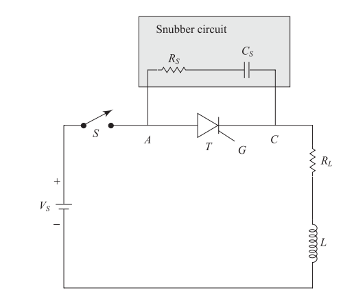
Snubber Circuit Analysis and Design
Circuit Analysis:
Design Equations:
-
Maximum current rate: \(\left. \frac{di}{dt} \right|_{\text{max}} = \frac{V_s}{L}\)
-
Snubber parameters: \(R = 2\zeta \sqrt{\frac{L}{C}}\), where \(\zeta = 0.5\)–1 (damping factor)
-
Capacitance: \(C = \frac{1 - \zeta^2}{L \left( \frac{dv}{dt} \right)_{\text{max}}^2}\)
Design Example:
-
Peak voltage: \(220\sqrt{2}\) V, Peak current: 100 A
-
\(\left. \frac{dv}{dt} \right|_{\text{max}} = 400\) V/\(\mu\)s, \(\left. \frac{di}{dt} \right|_{\text{max}} = 80\) A/\(\mu\)s
-
Safety factor: 2, Minimum \(R = 20\) \(\Omega\)
Design Considerations
Include safety factors and account for component tolerances in final design
Applications and Device Comparison
Power Conversion Systems:
-
AC-DC Rectifiers (Controlled rectification)
-
AC Controllers (Voltage/power control)
-
DC Choppers (DC-DC conversion)
-
Cycloconverters (Frequency conversion)
-
Static Switches (Contactless switching)
Industrial Applications:
-
Motor speed control drives
-
Electric furnace control
-
Welding power supplies
-
UPS systems
-
Battery chargers
High-Power Systems:
-
HVDC transmission systems
-
Flexible AC transmission (FACTS)
-
Wind turbine converters
-
Electric arc furnaces
-
Electrochemical processes
Selection Criteria:
-
Power rating \(>\) 10 kW
-
Switching frequency \(<\) 1 kHz
-
Cost-sensitive applications
-
High reliability requirements
-
Harsh operating environments
Market Position: Dominant in high-power, low-frequency applications
| Parameter | Thyristor | MOSFET | IGBT | BJT |
|---|---|---|---|---|
| Voltage Rating | \(>\)10 kV | \(<\)2 kV | \(<\)7 kV | \(<\)2 kV |
| Current Rating | \(>\)5 kA | \(<\)1 kA | \(<\)3 kA | \(<\)1 kA |
| Switching Freq | \(<\)1 kHz | \(>\)100 kHz | \(<\)50 kHz | \(<\)10 kHz |
| Gate Turn-off | No | Yes | Yes | Yes |
| On-state Loss | Lowest | Low | Medium | High |
| Drive Complexity | Low | Lowest | Medium | High |
| Cost (Relative) | 1 | 2–3 | 2–4 | 1–2 |
Device Selection Guidelines
Choose Thyristors for:
-
High power (\(>\)10 kW)
-
Low frequency (\(<\)1 kHz)
-
Cost-sensitive applications
-
High reliability requirements
-
Simple control schemes
Avoid Thyristors for:
-
High-frequency switching
-
Frequent ON/OFF control
-
Low power applications
-
Complex PWM control
-
Fast dynamic response
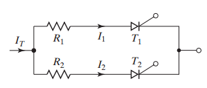
Series and Parallel Operation
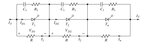
Design equation:
where \(\Delta I_{\mathrm{D}}\) = leakage current spread
Design Challenges:
-
Device characteristics vary due to manufacturing tolerances
-
Unequal voltage sharing can cause catastrophic device failure
-
Temperature variations significantly affect leakage currents
-
Dynamic voltage sharing during switching transients
Resistive Voltage Sharing Solution:
-
Equal resistors across each thyristor force voltage distribution
-
Resistance selection: \(R = \frac{V_{\mathrm{rated}}}{10 \times I_{\mathrm{leakage}(\max)}}\)
-
Continuous power dissipation trade-off
-
Additional RC snubbers for dynamic sharing
Derating Factor
Resistive Current Sharing:
-
Simple and reliable implementation
-
Excellent current sharing accuracy
-
Continuous conduction power loss
-
Resistance: \(R_{\mathrm{s}} = \frac{\Delta V_{\mathrm{on}}}{I_{\mathrm{rated}}}\)
Power Loss: \(P_{\mathrm{R}} = I^2 R_{\mathrm{s}}\)
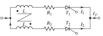
Magnetic Coupling Method:
-
Significantly lower conduction losses
-
Automatic current balancing mechanism
-
Fast response to current imbalances
-
More complex design requirements
-
Higher initial cost investment
Critical Requirements
- Common heat sink essential for thermal stability
-
Matched device characteristics preferred
-
Synchronized gate drive signals
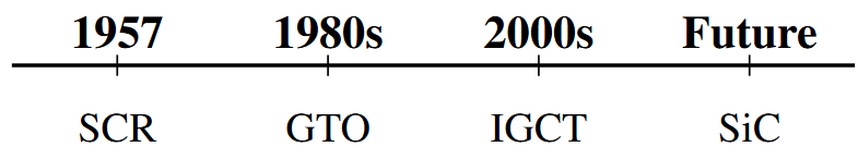
Advanced Topics and Future Trends
Enhanced Control Devices:
-
GTO (Gate Turn-Off): Gate controllable turn-off
-
MCT (MOS-Controlled): MOSFET-based gate drive
-
IGCT (Integrated Gate Commutated): High-power switching
-
ETO (Emitter Turn-Off): Advanced control features
Specialized Applications:
-
TRIAC: Bidirectional AC control
-
RCT: Reverse Conducting Thyristor
-
LTT: Light-Triggered Thyristor
-
BCT: Bidirectional Control Thyristor
Performance Enhancements:
-
Faster turn-off times (\(<\) 10 \(\mu\)s)
-
Higher \(\frac{\mathrm{d}v}{\mathrm{d}t}\) immunity ( \(>\) 1000 V/\(\mu\)s)
-
Integrated protection features
-
Improved thermal performance
-
Lower on-state voltage drop
Future Technology Trends:
-
SiC Thyristors: Higher temperature operation
-
Smart Power Modules: Integrated control electronics
-
Wide Bandgap: Enhanced performance characteristics
-
AI-Enhanced Control: Predictive switching algorithms
Conclusion
Fundamental Characteristics
- PNPN structure with regenerative switching mechanism
-
Gate triggering provides precise timing control
-
Latching behavior enables self-sustaining conduction
-
High power capability makes it industry standard
Design Essentials
- Protection against \( \frac{\mathrm{d}v}{\mathrm{d}t} \) and \( \frac{\mathrm{d}i}{\mathrm{d}t} \) effects
-
Thermal management is absolutely critical
-
Series/parallel operation needs careful design
-
Gate drive circuit reliability is essential
Performance Parameters
- Voltage ratings: Up to 12 kV
-
Current ratings: Up to 6 kA
-
Turn-on time: 1–6 \(\mu\)s
-
Turn-off time: 15–80 \(\mu\)s
Applications Summary
-
Power conversion systems
-
Industrial motor drives
-
HVDC transmission systems
-
Electric furnace control