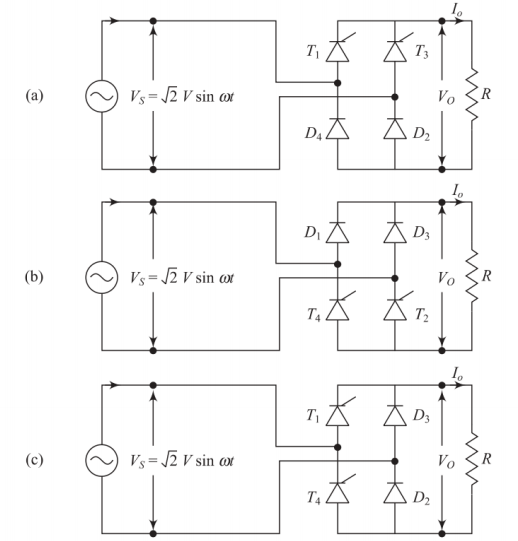
Single-Phase Half-Controlled Bridge Rectifier with R Load
Circuit Configuration
Key Features
-
Formed by replacing two thyristors of a full converter with diodes
-
Cost-effective solution with reduced control complexity
Configuration Types:
-
Symmetrical configurations:
-
Common cathode
-
Common anode
-
-
Asymmetrical configurations
Advantages:
-
Common cathode type most commonly used
-
Single triggering circuit for both thyristors
-
Simplified control scheme
Operation Principle
Positive Half Cycle
-
Thyristor \(T_1\) is forward biased
-
At \(\omega t = \alpha\): triggering pulse applied
-
\(T_1\) turns ON, current flows through \(T_1\) and \(D_2\)
-
At \(\omega t = \pi\): \(T_1\) reverse biased and turns OFF
Negative Half Cycle
-
Thyristor \(T_3\) is forward biased
-
At \(\omega t = \pi + \alpha\): triggering pulse applied
-
\(T_3\) turns ON, current flows through \(T_3\) and \(D_4\)
-
At \(\omega t = 2\pi\): \(T_3\) reverse biased and turns OFF
Key Point
Each thyristor conducts for \((\pi - \alpha)\) duration per cycle
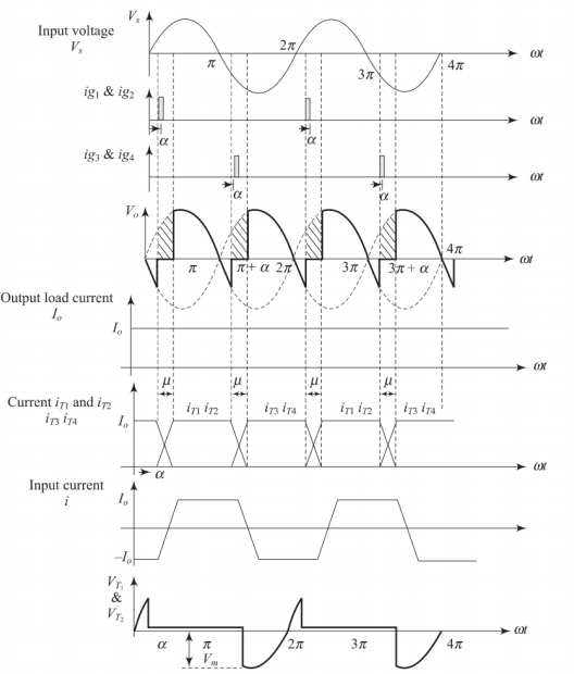
Voltage and Current Waveforms
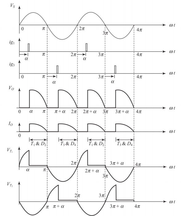
Waveform Characteristics
-
positive half-cycles
Output voltage waveform consists of of input voltage
-
Load current waveform follows voltage waveform (resistive load)
-
Conduction periods:
-
\(T_1\): \(\alpha\) to \(\pi\) in positive half cycle
-
\(T_3\): \(\pi + \alpha\) to \(2\pi\) in negative half cycle
-
Performance Parameters
Average Output Voltage:
Average Load Current:
RMS Output Voltage:
RMS Output Current:
Quality Factors
Form Factor:
Ripple Factor:
Note
-
Form factor increases with firing angle \(\alpha\)
-
Higher ripple factor indicates more AC content in output
Single-Phase Half-Controlled Bridge Rectifier with RL Load
Circuit Configuration and Key Differences
Configuration Types
Similar to R load case: Common cathode, Common anode, Asymmetrical
Impact of Inductance
-
Load current continues to flow at the end of each half cycle
-
Freewheeling action occurs through diodes
-
Current cannot change instantaneously due to \(L\frac{di}{dt}\) constraint
Operation Principle - Detailed Analysis
Positive Half Cycle (\(\alpha < \omega t < \pi\))
-
Thyristor \(T_1\) and diode \(D_2\) conduct
-
Supply voltage directly connected across load
-
Current builds up according to RL circuit dynamics
Freewheeling Period (\(\pi < \omega t < \pi + \alpha\))
-
Input voltage becomes negative, but current cannot reverse instantly
-
Diode \(D_1\) comes into conduction (freewheeling)
-
Load current flows through \(T_1\) and \(D_1\)
-
Current decays exponentially with time constant \(\tau = L/R\)
Negative Half Cycle (\(\pi + \alpha < \omega t < 2\pi\))
-
Thyristor \(T_3\) and diode \(D_4\) conduct
-
Process repeats for negative half cycle
Continuous vs Discontinuous Mode
Continuous Mode
-
Load current never reaches zero
-
Rectangular input current waveform
-
Magnitude equals load current during conduction
Discontinuous Mode
-
Load current reaches zero during each half cycle
-
Output voltage equals zero when current is zero
-
Conduction period depends on \(\tau = L/R\)
Performance Parameters for RL Load
Average Output Voltage:
RMS Output Voltage:
Important Note
For continuous conduction mode, voltage expressions remain same as R load case, but current analysis becomes more complex due to inductive effects.
Single-Phase Half-Controlled Bridge Rectifier with RLE Load
Circuit Configuration with Back EMF
Load Components
-
R: Resistance representing losses
-
L: Inductance providing current smoothing
-
E: Back EMF (e.g., from DC motor or battery)
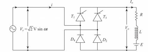
Operation Principle
-
Load current flows through either \(T_1\) or \(T_3\) and one diode
-
Positive half cycle: \(T_1\) and \(D_2\) conduct (\(\alpha < \omega t < \pi\))
-
Negative half cycle: \(T_3\) and \(D_4\) conduct (\(\pi + \alpha < \omega t < 2\pi\))
-
Freewheeling through \(T_1\) & \(D_1\) or \(T_3\) & \(D_3\)
Continuous Load Current Mode
Operating Conditions
Load current \(i_o\) is always greater than zero
Voltage Equation During Conduction:
Current Expression:
Continuous Mode Characteristics
Key Characteristics
-
Load current is continuous and always positive
-
Output voltage follows input voltage during thyristor conduction
-
Output voltage is zero during freewheeling periods
-
\(T_1\) conducts from \(\alpha\) until \(T_3\) is fired at \(\pi + \alpha\)
Discontinuous Load Current Mode
Operating Conditions
Load current \(i_o\) becomes zero for certain time periods
Operation Sequence
-
When \(T_1\) triggered at \(\omega t = \alpha\) and output voltage \(>\) E:
-
Current starts from zero and increases
-
Current increases until \(\omega t = \pi - \theta\) (where output voltage = E)
-
After \(\omega t = \pi - \theta\): output voltage \(<\) E, current decreases
-
At \(\omega t = \beta\): current becomes zero before \(T_3\) is triggered
-
-
During \(\beta < \omega t < \pi + \alpha\):
-
No devices conduct
-
Output voltage equals back EMF E
-
Discontinuous Mode Waveforms
Important Observations
-
Load current starts and ends at zero during each half cycle
-
Output voltage equals back EMF E when no devices conduct
-
Conduction angle \(\gamma = \beta - \alpha\) depends on:
-
Firing angle \(\alpha\)
-
Load parameters (R, L, E)
-
Input voltage magnitude
-
Performance Analysis with High Inductive Load
High Inductance Approximation
Assumptions
When inductance is very high: load current is continuous with negligible ripple
Input Current Expression:
Fourier Series Representation:
RMS Fundamental Current:
Power Quality Parameters
Displacement Factor:
Distortion Factor:
Power Factor:
Harmonic Factor:
Power Analysis
Active Input Power:
Reactive Power Input:
Power Factor Implications
-
Power factor decreases as firing angle \(\alpha\) increases
-
At \(\alpha = 0^{\circ}\): Maximum power factor = \(\frac{2\sqrt{2}}{\pi} \approx 0.9\)
-
At \(\alpha = 90^{\circ}\): Power factor = \(\frac{\sqrt{2}}{\pi} \approx 0.45\)
Centre Tap Transformer with Leakage Inductance
Effect of Transformer Leakage Inductance
Circuit Components
-
Centre tap transformer with leakage inductance \(L_c\)
-
RL load
-
Two thyristors
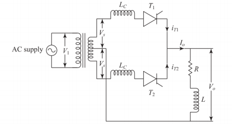
Commutation Process
-
Current cannot transfer instantaneously between thyristors
-
Finite commutation time required
-
Commutation overlap interval (\(u\)) occurs
-
During overlap: both thyristors conduct simultaneously
Physical Interpretation
Leakage inductance opposes sudden current changes, causing gradual transfer of current from outgoing to incoming thyristor.
Commutation Analysis
Commutation Process
-
Initially: one thyristor conducts full load current
-
At \(\omega t = \alpha\): second thyristor is triggered
-
During overlap (\(\alpha\) to \(\alpha + u\)):
-
Both thyristors conduct
-
Current transfers gradually from first to second thyristor
-
Short circuit occurs in transformer secondary
-
-
At \(\omega t = \alpha + u\): commutation complete
Overlap Angle Relationship:
Voltage Reduction Due to Commutation
Voltage Drop During Commutation:
Actual Average Output Voltage:
Key Insights
-
Average output voltage is reduced by commutation reactance
-
Voltage drop is proportional to load current
-
Higher leakage inductance \(\Rightarrow\) greater voltage drop
Bridge Rectifier with Source Inductance
Full-Wave Controlled Bridge with Source Inductance
Configuration
-
Four thyristors in bridge configuration
-
RL load with source inductance \(L_s\)
-
Assumptions: continuous conduction, ripple-free load current
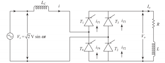
Source Inductance Effects
-
Output voltage not constant during conduction
-
Input current waveform changes significantly
-
Commutation overlap occurs between thyristor pairs
Commutation Process in Bridge Rectifier
Commutation Sequence
-
Initially: \(T_3\) and \(T_4\) conduct
-
At \(\omega t = \alpha\): \(T_1\) and \(T_2\) are triggered
-
During overlap (\(\alpha\) to \(\alpha + u\)):
-
All four thyristors conduct
-
Load current freewheels through all devices
-
Output voltage becomes zero
-
Input current changes polarity gradually
-
-
At \(\omega t = \alpha + u\): \(T_3\) and \(T_4\) turn OFF
Mathematical Analysis of Commutation
Voltage Equation During Overlap:
Current During Overlap:
Overlap Angle:
Corrected Average Output Voltage:
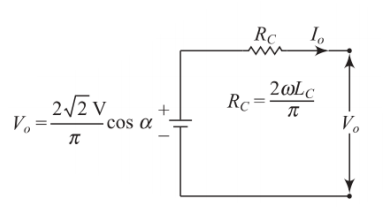
Equivalent Circuit Model
Simplified Model
-
DC voltage source: \(\frac{2\sqrt{2}V}{\pi} \cos\alpha\)
-
Commutation resistance: \(R_c = \frac{2\omega L_s}{\pi}\)
-
Series combination represents rectifier behavior
Physical Meaning
Commutation resistance represents:
-
Voltage drop across source inductance
-
Power loss during commutation
Waveforms with Source Inductance
Waveform Analysis
-
Input voltage: sinusoidal AC supply
-
Output voltage: reduced due to commutation overlap
-
Load current: continuous and smooth
-
Thyristor currents: show overlap periods
-
Input current: trapezoidal shape due to commutation
Performance Parameters of Controlled Rectifiers
Fundamental Performance Metrics
Rectification Efficiency: \(\eta = \frac{P_{dc}}{P_{ac}} \times 100\%\) where:
Form Factor: \(FF = \frac{V_{rms}}{V_{dc}}\) Voltage Ripple Factor: \(RF = \sqrt{FF^2 - 1}\)
Quality Indicators
-
Lower ripple factor indicates better DC quality
-
Higher efficiency indicates better power conversion
-
For ripple-free load current: \(CRF = 0\)
Power Factor Analysis
RMS Fundamental Current: \(I_1 = \frac{2\sqrt{2}I_a}{\pi\sqrt{1 + \cos\alpha}}\)
Displacement Factor: \(DF = \cos\phi_1 = \cos\left(\frac{\alpha}{2}\right)\)
Distortion Factor: \(CDF = \frac{2\sqrt{2}}{\pi\sqrt{1 + \cos\alpha}}\)
Overall Power Factor: \(PF = CDF \times DF\)
Power Components:
Comparative Analysis
Performance Comparison
| Parameter | R Load | RL Load | RLE Load |
|---|---|---|---|
| Average Voltage | \(\frac{\sqrt{2}V}{\pi}(1+\cos\alpha)\) | Same | Same |
| Current Mode | Discontinuous | Continuous/Disc. | Continuous/Disc. |
| Freewheeling | No | Yes | Yes |
| Back EMF Effect | No | No | Yes |
| Control Range | \(0^{\circ} \leq \alpha \leq 180^{\circ}\) | \(0^{\circ} \leq \alpha \leq 180^{\circ}\) | Limited by E |
Key Differences
-
R Load: Simplest analysis, current follows voltage
-
RL Load: Freewheeling improves current continuity
-
RLE Load: Back EMF limits control range and affects mode of operation
Design Considerations
Advantages
-
Reduced cost (fewer thyristors)
-
Simpler control circuitry
-
Natural freewheeling through diodes
-
Good performance for many applications
Limitations
-
Lower power factor compared to full-controlled
-
Higher harmonic content
-
Limited control range with back EMF loads
-
Voltage drop due to commutation inductance
Applications
-
DC motor drives with moderate performance requirements
-
Battery charging systems
-
DC power supplies with cost constraints
Summary and Conclusions
Key Takeaways
Circuit Configurations
-
Half-controlled bridge rectifiers use two thyristors + two diodes
-
Common cathode configuration most widely used
-
Different load types require different analytical approaches
Operating Characteristics
-
R Load: Current discontinuous, follows voltage waveform
-
RL Load: Freewheeling action, continuous/discontinuous modes possible
-
RLE Load: Back EMF affects conduction, mode depends on load parameters
Practical Considerations
-
Leakage/source inductance causes commutation overlap
-
Results in voltage reduction and altered current waveforms
-
Can be modeled using equivalent circuit with commutation resistance
Performance Summary
Critical Performance Metrics
-
Average output voltage: \(V_{dc} = \frac{\sqrt{2}V}{\pi}(1 + \cos\alpha)\)
-
Power factor: Decreases with increasing firing angle
-
Harmonic distortion: Significant due to non-sinusoidal input current
-
Commutation effects: Reduce output voltage by \(\frac{2\omega L I_a}{\pi}\)
Design Guidelines
-
Choose firing angle based on voltage regulation requirements
-
Consider power factor implications for AC supply
-
Account for commutation effects in practical designs
-
Use appropriate filtering for output ripple reduction