What is a Power MOSFET?
-
Power MOSFET: High-power version of conventional MOSFET
-
Designed to handle high voltages (up to several kV) and currents (hundreds of amperes)
-
Combines advantages of MOSFETs with power handling capability
-
Voltage-controlled device (unlike BJT which is current-controlled)
-
Dominant device in low to medium voltage power electronics
Key Applications:
-
Switch-mode power supplies (SMPS)
-
Motor drives and inverters
-
DC-DC converters
-
Automotive electronics
-
LED drivers
MOSFET Basics - Three Terminal Device
Three terminals:
-
Gate (G): Control terminal (analogous to base of BJT)
-
Drain (D): Output terminal (analogous to collector of BJT)
-
Source (S): Reference terminal (analogous to emitter of BJT)
Key Characteristics:
-
Current flow from drain to source controlled by gate-source voltage
-
High input impedance (M\(\Omega\))
-
Unidirectional current flow when ON
-
Can block voltage in only one direction when OFF
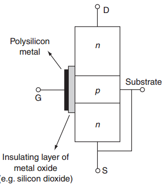
Power MOSFET Structure
Basic Structure:
-
n+ source region
-
p-type substrate (body)
-
n- drain region (lightly doped)
-
Metal gate electrode
-
Insulating oxide layer (SiO\(_2\))
Operation Principle:
-
Gate voltage creates electric field
-
Field attracts/repels charge carriers
-
Forms conducting channel
-
Controls current flow
Types of Power MOSFETs
1. Based on Channel Type:
-
N-channel MOSFET: More common, electrons are majority carriers
-
P-channel MOSFET: Holes are majority carriers, slower switching
2. Based on Operation Mode:
-
Enhancement Mode: Normally OFF, requires positive \(V_{GS}\) to turn ON
-
Depletion Mode: Normally ON, requires negative \(V_{GS}\) to turn OFF
3. Based on Construction:
-
VDMOS: Vertical Double-diffused MOS
-
UMOS: U-groove MOS structure
-
Trench MOSFET: Vertical trench gate structure
Note: Power MOSFETs are typically n-channel enhancement mode devices
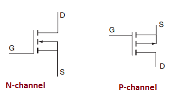
MOSFET Symbols and Body Diode
Symbol Convention:
-
N-channel: Arrow points inward (toward channel)
-
P-channel: Arrow points outward (away from channel)
-
Broken line: Enhancement mode (normally OFF)
-
Solid line: Depletion mode (rarely used)
Body Diode (Intrinsic Diode):
-
Parasitic diode between drain and source
-
Provides reverse current path
-
Useful in bridge circuits
-
Eliminates need for external freewheeling diode
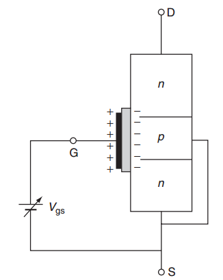
MOSFET Operation - Turn-ON Process
For N-channel Enhancement Mode MOSFET:
-
\(V_{GS} < V_{th}\): Device OFF
-
No conducting channel exists
-
Only leakage current flows (\(I_D \approx 0\))
-
-
\(V_{GS} = V_{th}\): Threshold condition
-
Threshold voltage (\(V_{th}\)): Typically 2-4V for power MOSFETs
-
Weak inversion begins
-
-
\(V_{GS} > V_{th}\): Channel formation
-
Electric field attracts electrons to surface
-
Forms n-type conducting channel
-
Current flows from drain to source
-
Higher \(V_{GS}\) \(\to\) wider channel \(\to\) more current
-
-
\(V_{GS} = 10-15V\): Full enhancement
-
Maximum channel conductivity
-
Minimum ON-resistance achieved
-
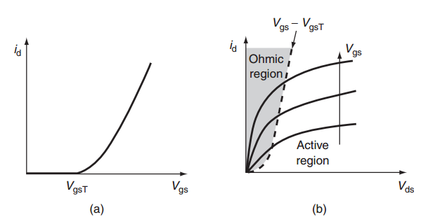
Operating Regions
1. Cut-off Region:
-
\(V_{GS} < V_{th}\)
-
\(I_D = 0\) (switch OFF)
2. Ohmic/Linear Region:
-
\(V_{DS} < (V_{GS} - V_{th})\)
-
Acts like voltage-controlled resistor
-
Used for switching (ON-state)
3. Saturation/Active Region:
-
\(V_{DS} > (V_{GS} - V_{th})\)
-
Acts like current source
-
Used for amplification
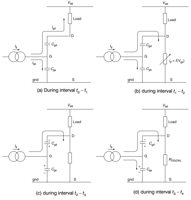
Equivalent circuits during turning ON of a MOSFET
Transfer Characteristics
Transfer Characteristic: \(I_D\) vs \(V_{GS}\) relationship
Key Parameters:
-
Threshold voltage (\(V_{th}\)): 2-4V typically
-
Transconductance (\(g_m\)):
\[g_m = \frac{\partial I_D}{\partial V_{GS}}\]
Square Law (in saturation):
where K is the transconductance parameter
ON-State Parameters
ON-state resistance (\(R_{DS(ON)}\)):
-
Drain-source resistance when MOSFET is fully ON
-
Most important parameter for device selection
-
Determines conduction losses: \(P_{cond} = I_D^2 \times R_{DS(ON)}\)
-
Specified at particular \(V_{GS}\) (typically 10V) and temperature ( \(25^{\circ}C\))
Gate Drive Voltage Guidelines:
-
\(V_{GS} = 10V\): Usually sufficient for most applications
-
\(V_{GS} = 15V\): Recommended for minimum \(R_{DS(ON)}\)
-
\(V_{GS(max)} = \pm 20V\): Absolute maximum (oxide breakdown limit)
Temperature Effects:
-
\(R_{DS(ON)}\) increases with temperature (\(\sim 0.6\%/^{\circ}C\))
-
\(V_{th}\) decreases with temperature (\(\sim -2mV/^{\circ}\)C)
-
Positive temperature coefficient helps in paralleling
Breakdown Characteristics
Voltage Ratings:
-
Drain-source breakdown (\(BV_{DSS}\)):
-
Maximum \(V_{DS}\) when device is OFF
-
Range: 50V to several kV
-
Choose 2-3 times operating voltage
-
Avalanche breakdown in drain region
-
-
Gate-source breakdown (\(BV_{GSS}\)):
-
Maximum \(V_{GS}\) without oxide damage
-
Typically \(\pm 20V\) to \(\pm 30V\)
-
Critical: Permanent damage if exceeded
-
Very thin oxide layer ( 100 nm)
-
Safe Operating Area (SOA):
-
Defines safe current-voltage operating limits
-
Limited by: current, voltage, power, and thermal constraints
-
Advantage: No secondary breakdown (unlike BJTs)
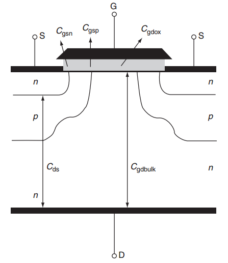
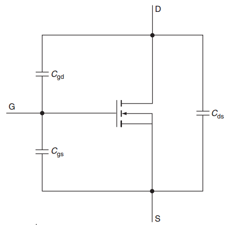
Parasitic Capacitances
Main Capacitances:
-
\(C_{GS}\): Gate-source capacitance
-
\(C_{GD}\): Gate-drain capacitance (Miller)
-
\(C_{DS}\): Drain-source capacitance
Datasheet Parameters:
-
\(C_{ISS} = C_{GS} + C_{GD}\) (Input)
-
\(C_{OSS} = C_{DS} + C_{GD}\) (Output)
-
\(C_{RSS} = C_{GD}\) (Reverse transfer)
Impact:
-
Determine switching speeds
-
\(C_{GD}\) creates Miller effect
-
All are voltage-dependent
Body Diode Characteristics
Body Diode Properties:
-
Inherent p-n junction between drain and source
-
Always present in power MOSFETs
-
Forward voltage drop: 0.7-1.2V (similar to regular diode)
-
Reverse recovery time: typically slow (\(100~\mathrm{ns} - 1~\mathrm{\mu s}\))
Advantages:
-
Provides freewheeling path for inductive loads
-
Eliminates need for external diode in many circuits
-
Enables bidirectional current flow
-
Useful in bridge circuits and motor drives
Disadvantages:
-
Slow reverse recovery can cause losses
-
Higher forward drop compared to dedicated diodes
-
May require external fast diode in high-frequency applications
Switching Behavior Overview
Why Study Switching?
-
Power MOSFETs used primarily as switches
-
Switching losses significant at high frequencies
-
Switching speed determines maximum operating frequency
-
Critical for gate drive circuit design
MOSFET Switching Advantages:
-
Majority carrier device: No stored charge
-
No storage time: Unlike BJTs
-
Fast switching: Limited only by capacitances
-
Voltage controlled: No continuous gate current
Switching Limitations:
-
Parasitic capacitances must be charged/discharged
-
Miller effect during transitions
-
Gate drive capability requirements
Switching Time Definitions
Turn-ON Times:
-
\(t_{d(on)}\): Turn-on delay time
-
\(t_r\): Current rise time (10% to 90%)
-
\(t_{on} = t_{d(on)} + t_r\): Total turn-on time
Turn-OFF Times:
-
\(t_{d(off)}\): Turn-off delay time
-
\(t_f\): Current fall time (90% to 10%)
-
\(t_{off} = t_{d(off)} + t_f\): Total turn-off time
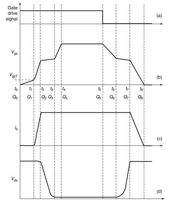
Factors Affecting Switching Speed:
-
Gate drive current capability
-
Parasitic capacitances (especially \(C_{GD}\))
-
Gate resistance
-
Load characteristics
Miller Effect and Gate Charge
Miller Effect:
-
Caused by gate-drain capacitance (\(C_{GD}\))
-
Creates plateau in gate voltage during switching
-
Slows down switching transitions
-
Duration: \(t_{miller} = \frac{C_{GD} \times \Delta V_{DS}}{I_{gate}}\)
Gate Charge (\(Q_G\)):
-
Total charge needed to turn MOSFET ON
-
More practical parameter than capacitances
-
Independent of gate drive voltage (approximately)
-
\(Q_G = Q_{GS} + Q_{GD}\) (gate-source + gate-drain charge)
Switching Time with Constant Current Drive:
Gate Drive Circuit Requirements
Why Proper Gate Drive is Critical:
-
MOSFET performance depends on gate drive quality
-
Poor gate drive \(\to\) slow switching \(\to\) high losses
-
Must provide sufficient voltage and current
Key Requirements:
-
Voltage: 10-15V for full enhancement
-
Current capability: To charge gate capacitances quickly
-
Low impedance: Minimize gate resistance
-
Fast rise/fall times: For high-frequency operation
-
Isolation: For high-side switches
-
Protection: Against gate overvoltage
Gate Resistance Guidelines:
-
Lower \(R_G\): Faster switching, higher peak currents, more EMI
-
Higher \(R_G\): Slower switching, reduced EMI, prevents oscillations
-
Typical range: \(10-100~\Omega\)
Gate Drive Circuit Types
1. Direct Drive:
-
From logic gates or microcontrollers
-
Only for small MOSFETs with low gate charge
-
Limited current capability
2. Bipolar Transistor Drivers:
-
Push-pull configuration (NPN + PNP)
-
Higher current capability
-
Discrete component approach
3. Dedicated Gate Driver ICs:
-
Optimized for MOSFET driving
-
Features: dead-time, shoot-through protection, UVLO
-
Examples: IR2110, TC4427, MCP1416
4. Transformer-Coupled Drivers:
-
Provides galvanic isolation
-
Good for high-voltage applications
-
More complex circuit
Types of Power Losses
1. Conduction Losses:
2. Switching Losses:
3. Gate Drive Losses:
4. Body Diode Conduction Losses:
Thermal Management
Thermal Resistance Model:
Heat Sink Design:
where:
-
\(T_j\): Junction temperature (max \(150-175^{\circ}C\))
-
\(T_a\): Ambient temperature
-
\(\theta_{jc}\): Junction-to-case thermal resistance
-
\(\theta_{cs}\): Case-to-sink thermal resistance
-
\(\theta_{sa}\): Sink-to-ambient thermal resistance
Thermal Management Tips:
-
Use adequate heat sink area
-
Apply thermal interface material properly
-
Consider forced air cooling for high power
-
Derate current at high temperatures
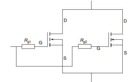
Paralleling Power MOSFETs
Why Parallel MOSFETs?
-
Increase current capability
-
Reduce ON-resistance
-
Better thermal distribution
-
Cost-effective solution
-
Enhanced reliability
Advantages Over BJTs:
-
Positive temperature coefficient
-
Self-balancing current sharing
-
No current sharing resistors needed
-
No thermal runaway
Current Sharing Mechanism:
-
Device carrying more current heats up
-
Higher temperature \(\to\) Higher \(R_{DS(ON)}\)
-
Higher resistance \(\to\) Current reduces automatically
-
Natural negative feedback mechanism
MOSFET vs BJT - Comprehensive Comparison
| Parameter | Power MOSFET | Power BJT |
|---|---|---|
| Control method | Voltage controlled | Current controlled |
| Input impedance | Very high (\(M\Omega\)) | Medium (\(k\Omega\)) |
| Drive power | Very low | Higher |
| Switching speed | Fast (10-100 ns) | Slower (\(1-10 ~\mathrm{\mu s}\)) |
| ON-state voltage drop | Higher (\(I \times R_{DS(ON)}\)) | Lower (\(V_{CE(sat)}\)) |
| Secondary breakdown | Not applicable | Possible |
| Thermal runaway | No | Yes |
| Paralleling | Easy (self-balancing) | Difficult |
| Temperature coefficient | Positive (\(R_{DS(ON)}\)) | Negative |
| Frequency capability | Higher | Lower |
| Cost per ampere | Higher | Lower |
| Voltage capability | Limited \((\sim1000~\mathrm{V}\)) | Higher (\(>1000~\mathrm{V}\)) |
MOSFET Selection Criteria
1. Voltage Rating (\(V_{DSS}\)):
-
Choose 2-3 times maximum operating voltage
-
Account for voltage spikes and transients
-
Consider derating with temperature
2. Current Rating (\(I_D\)):
-
Based on RMS current (for resistive loads)
-
Consider peak current capability
-
Account for thermal limitations
3. ON-Resistance (\(R_{DS(ON)}\)):
-
Lower resistance = lower conduction losses
-
Specified at \(V_{GS} = 10V\), \(T = 25^{\circ}C\)
-
Consider temperature rise effect
4. Switching Parameters:
-
Gate charge (\(Q_G\)) for switching losses
-
Gate capacitances for drive circuit design
-
Rise/fall times for frequency capability
Applications of Power MOSFETs
1. Switch-Mode Power Supplies (SMPS):
-
Buck, boost, buck-boost converters
-
Forward, flyback converters
-
Resonant converters
2. Motor Drives:
-
Three-phase inverters
-
Servo drives
-
Stepper motor drivers
3. Automotive Electronics:
-
Electronic ignition systems
-
Fuel injection control
-
Electric power steering
4. Other Applications:
-
LED lighting drivers
-
Battery management systems
-
Solar inverters
-
Audio amplifiers
MOSFET Protection
Protection Requirements:
-
Overcurrent: Excessive drain current
-
Overvoltage: \(V_{DS}\) exceeding \(BV_{DSS}\)
-
Gate overvoltage: \(V_{GS}\) exceeding \(\pm 20V\)
-
Thermal: Junction temperature exceeding limits
-
dv/dt: Fast voltage transitions causing unwanted turn-on
Protection Methods:
-
Snubber circuits: RC or RCD networks
-
Gate clamping: Zener diodes across gate-source
-
Current sensing: Shunt resistors or current transformers
-
Thermal shutdown: Temperature monitoring
Layout Considerations:
-
Minimize parasitic inductances
-
Keep gate drive traces short
-
Use ground planes effectively
Practical Design Considerations
Gate Drive Design:
-
Use separate turn-on and turn-off gate resistors if needed
-
Consider gate drive power supply decoupling
-
Implement dead-time in bridge circuits
-
Use negative gate drive voltage for better turn-off
PCB Layout Guidelines:
-
Keep power loop area minimal
-
Use thick traces for high current paths
-
Place gate drive close to MOSFET
-
Use via stitching for thermal management
Common Design Pitfalls:
-
Inadequate gate drive current
-
Poor thermal design
-
Ignoring parasitic inductances
-
Insufficient protection circuitry
Advanced MOSFET Technologies
1. SiC (Silicon Carbide) MOSFETs:
-
Higher voltage capability (\(>1200~\mathrm{V}\))
-
Lower ON-resistance
-
Higher temperature operation (\(200^{\circ}C\))
-
Faster switching speeds
-
Higher cost but improving efficiency
2. GaN (Gallium Nitride) HEMTs:
-
Ultra-fast switching (sub-nanosecond)
-
Very low gate charge
-
High frequency capability (MHz range)
-
No body diode (can be advantage or disadvantage)
3. Superjunction MOSFETs:
-
Overcome silicon limit of \(R_{DS(ON)}\) vs voltage rating
-
Better figure of merit
-
Complex manufacturing process
Summary
Key Takeaways:
-
Power MOSFETs are voltage-controlled, majority carrier devices
-
Excellent for switching applications due to fast switching
-
Three main operating regions: cut-off, ohmic, and saturation
-
ON-resistance is the most critical parameter for power applications
-
Proper gate drive is essential for optimal performance
-
Natural current sharing makes paralleling straightforward
Advantages:
-
High input impedance, low drive power
-
Fast switching, no storage time
-
Positive temperature coefficient, no thermal runaway
-
Easy to parallel, robust operation
Applications: Dominant in low-to-medium voltage power electronics, especially where high switching frequency is required.
Future Trends
Technology Evolution:
-
Wide bandgap semiconductors (SiC, GaN) gaining market share
-
Integration with smart gate drivers
-
Advanced packaging for better thermal performance
-
Higher voltage silicon MOSFETs with superjunction technology
Application Trends:
-
Electric vehicles driving demand for high-efficiency devices
-
Renewable energy systems requiring robust switching
-
Data center power supplies demanding higher efficiency
-
Wireless power transfer applications
The future belongs to wide bandgap semiconductors, but silicon MOSFETs will remain important for cost-sensitive applications.