Learning Objectives
By the end of this lecture, you will be able to:
-
Understand the structure and operation of power BJTs
-
Analyze static and dynamic characteristics
-
Design appropriate base drive circuits
-
Apply thermal management principles
-
Compare power BJTs with other switching devices
-
Select power BJTs for specific applications
What is a Power BJT?
-
Definition: Bipolar Junction Transistor optimized for high-power switching and amplification
-
Power Ratings:
-
Voltage: 50 V to 1500 V
-
Current: 1 A to 500 A+
-
Power: Up to several kW
-
-
Key Differences from small-signal BJTs:
-
Larger die size
-
Enhanced thermal packaging
-
Optimized for switching applications
-

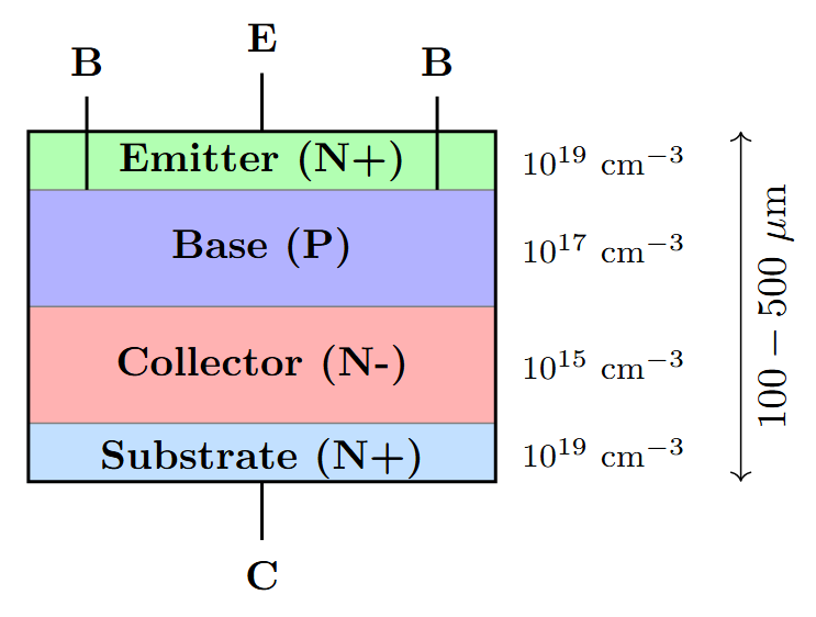
Structure of Power BJTs
Key Structural Features:
-
Emitter: Heavily doped (N+ or P+)
-
Base: Thin, lightly doped
-
Collector: Thick, lightly doped for high voltage
-
Epitaxial Layer: For voltage blocking
-
Substrate: Heavily doped for low resistance
Package Types:
-
TO-3, TO-218, TO-247
-
Module packages
-
Press-pack assemblies
Operation Modes of Power BJTs
-
Cut-off Mode
-
\(V_{BE} < V_{BE(\text{th})} \approx {0.7}{~\mathrm{V}}\)
-
\(I_B = 0\), \(I_C \approx I_{CBO}\) (leakage)
-
Transistor acts as open switch
-
-
Active Mode
-
\(V_{BE} > {0.7}{~\mathrm{V}}\), \(V_{CE} > V_{CE(\text{sat})}\)
-
\(I_C = \beta I_B\)
-
Linear amplification region
-
-
Saturation Mode
-
High \(I_B\), \(V_{CE} < V_{CE(\text{sat})}\)
-
\(I_C < \beta I_B\) (current limited by load)
-
Transistor acts as closed switch
-
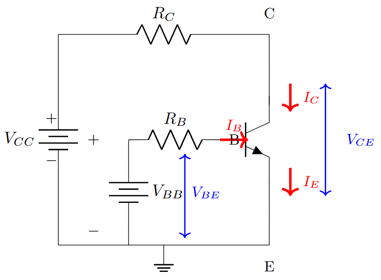
Current Relationships and Parameters
Basic Relationships:
Typical Power BJT Parameters:
-
\(\beta = 10\)–\(100\) (lower than small-signal)
-
\(V_{BE(\text{on})} = {0.7}{~\mathrm{V}}\)–\({1.5}{~\mathrm{V}}\)
-
\(V_{CE(\text{sat})} = {0.2}{~\mathrm{V}}\)–\({2}{~\mathrm{V}}\)
-
\(I_{CBO} < {1}{~\mathrm{mA}}\) (at 25 °C)
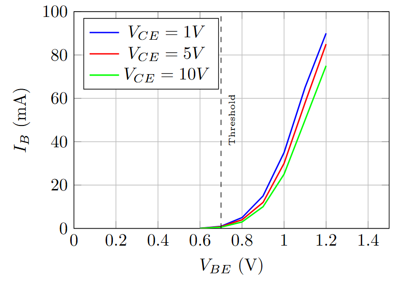
Input Characteristics (\(V_{BE}\) vs \(I_B\))
Key Features:
-
Exponential relationship (diode-like)
-
\(I_B = I_S e^{V_{BE}/V_T}\)
-
Temperature dependent
-
\(V_{BE}\) decreases \(\sim 2~\mathrm{mV^{\circ}C^{-1}}\)
-
Different for various \(V_{CE}\) values
Practical Implications:
-
Base drive design critical
-
Temperature compensation needed
-
Current limiting resistors required
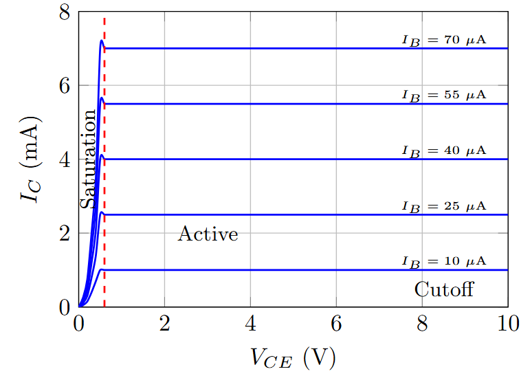
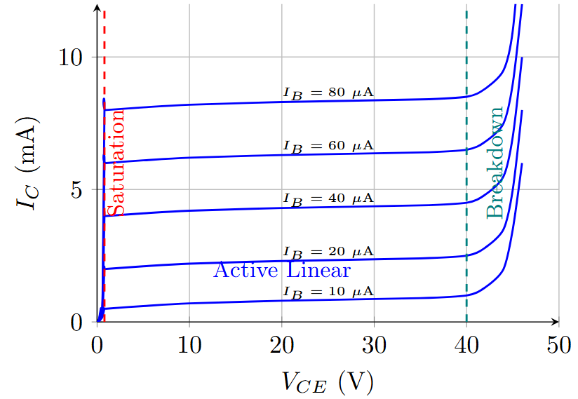
Output Characteristics (\(I_C\) vs \(V_{CE}\))
Regions Analysis:
-
Saturation (\(V_{CE} < {1}{~\mathrm{V}}\)):
-
Steep rise in \(I_C\)
-
Low \(V_{CE(\text{sat})}\) desirable
-
Switching applications
-
-
Active (\(V_{CE} > {1}{~\mathrm{V}}\)):
-
Constant \(I_C\) for given \(I_B\)
-
\(I_C = \beta I_B\)
-
Slight positive slope (Early effect)
-
-
Breakdown:
-
\(V_{CE} > BV_{CEO}\)
-
Avalanche multiplication
-
Destructive if not current limited
-
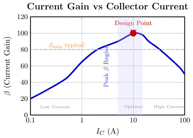
Transfer Characteristics and Key Parameters
DC Current Gain (\(\beta\) or \(h_{FE}\)):
-
\(\beta = \frac{I_C}{I_B}\) (in active region)
-
Varies with \(I_C\), \(V_{CE}\), and temperature
-
Typically 20–100 for power BJTs
-
Design for worst-case minimum \(\beta\)
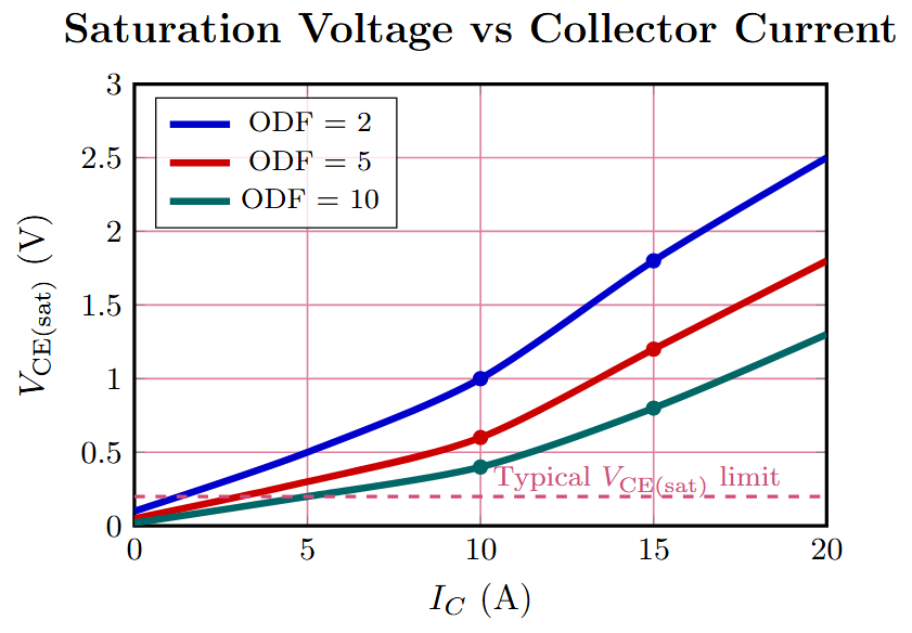
Saturation Parameters:
-
\(V_{CE(\text{sat})}\): Collector-emitter saturation voltage
-
\(V_{BE(\text{sat})}\): Base-emitter saturation voltage
-
Overdrive factor: \(\text{ODF} = \frac{I_B}{I_{B(\text{min})}}\)
-
Typical: \(V_{CE(\text{sat})} = {0.2}{~\mathrm{V}}\)–\({2}{~\mathrm{V}}\)
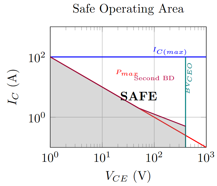
Safe Operating Area (SOA) – Concept
Definition:
-
Region of \(V_{CE}\) vs \(I_C\) where device operates safely
-
Bounded by multiple failure mechanisms
-
Critical for reliability and device protection
Limiting Factors:
-
Maximum Current: Bondwire/metallization limits
-
Power Dissipation: Thermal limits
-
Voltage Breakdown: \(BV_{CEO}\)
-
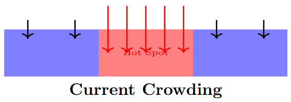
Second Breakdown: Current crowding
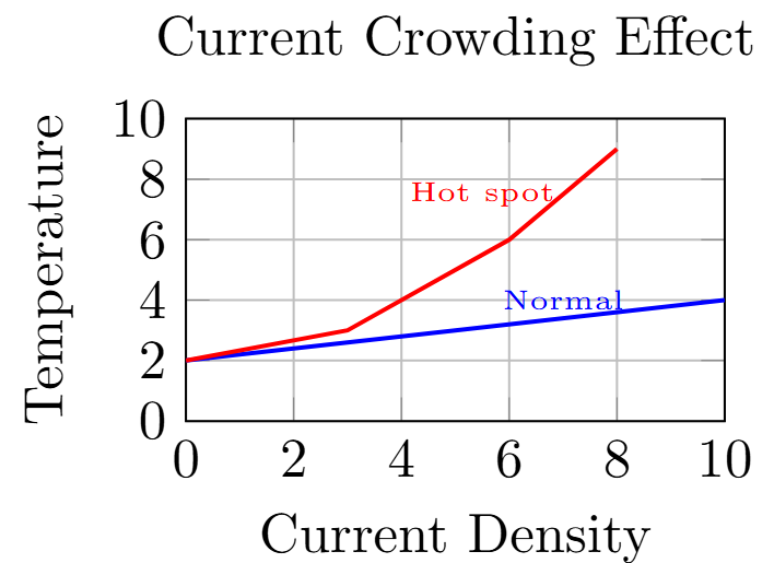
Second Breakdown Phenomenon
Mechanism:
-
Current crowding due to negative temperature coefficient
-
Hot spots form \(\rightarrow\) local current increase
-
Positive feedback \(\rightarrow\) thermal runaway
-
Occurs at high \(V_{CE}\) and moderate \(I_C\)
Prevention Methods:
-
Interdigitated emitter design
-
Ballasting resistors
-
Current sharing circuits
-
Proper thermal management
-
Stay within FBSOA limits
Switching Behavior Overview
Key Challenges:
-
Minority carrier storage in base
-
Charge removal during turn-off
-
Slow switching compared to MOSFETs
-
Turn-off time \(\gg\) Turn-on time
Switching Times:
-
\(t_d\): Delay time (10 ns–50 ns)
-
\(t_r\): Rise time (50 ns–200 ns)
-
\(t_s\): Storage time (100 ns–500 ns)
-
\(t_f\): Fall time (50 ns–200 ns)
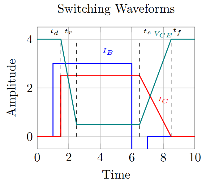
Turn-On Process Analysis
Phase 1: Delay Time (\(t_d\))
-
Base-emitter junction charging
-
\(V_{BE}\) rises from 0 to \(V_{BE(\text{th})}\)
-
No collector current flows
-
\(t_d \approx \tau_B \ln\left(\frac{V_{BB}}{V_{BB} - V_{BE(\text{th})}}\right)\)
Phase 2: Rise Time (\(t_r\))
-
Collector current rises exponentially
-
\(V_{CE}\) begins to fall
-
Active region operation
-
\(t_r \approx \tau_B \ln\left(\frac{I_{C(\text{final})}}{0.1 \cdot I_{C(\text{final})}}\right)\)
Equivalent Circuit During Turn-On:
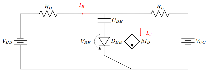
Time Constants:
Turn-Off Process Analysis
Phase 1: Storage Time (\(t_s\))
-
Excess base charge removal
-
\(I_C\) remains constant
-
\(V_{CE}\) remains at \(V_{CE(\text{sat})}\)
-
Dominated by minority carrier lifetime
-
\(t_s = \tau_s \ln\left(\frac{I_{B(\text{on})} + I_{B(\text{off})}}{I_{B(\text{off})}}\right)\)
Phase 2: Fall Time (\(t_f\))
-
\(I_C\) decreases exponentially
-
\(V_{CE}\) rises to \(V_{CC}\)
-
Transistor enters cut-off
-
\(t_f \approx \tau_B \ln(9)\) (90% to 10%)
Charge Control Model:
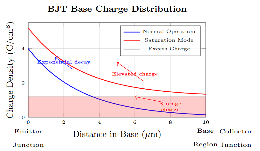
Storage Time Constant:
Switching Losses
Turn-On Loss:
Turn-Off Loss:
Total Switching Power:
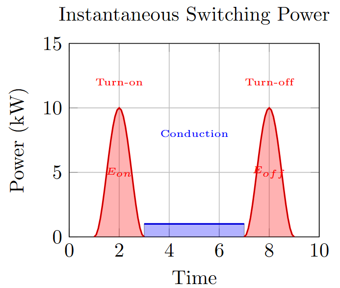
Typical Values:
-
Turn-on time: 100 ns–300 ns
-
Turn-off time: 1 μs–5 μs
-
Storage time dominates turn-off
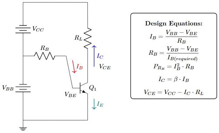
Base Drive Requirements
Turn-On Requirements:
-
Sufficient base current: \(I_{B(\text{on})} \geq \frac{I_C}{\beta_{\text{min}}}\)
-
Overdrive for fast turn-on: \(I_{B(\text{on})} = \text{ODF} \times I_{B(\text{min})}\)
-
Typical ODF = 2–10
-
Low impedance drive source
Turn-Off Requirements:
-
Negative base current for fast turn-off
-
\(I_{B(\text{off})} = -I_{B(\text{on})}/2\) (typical)
-
Low impedance path for charge removal
-
Reverse base-emitter voltage if needed
Basic Resistive Drive:
Advanced Base Drive Circuits
Push-Pull Drive:
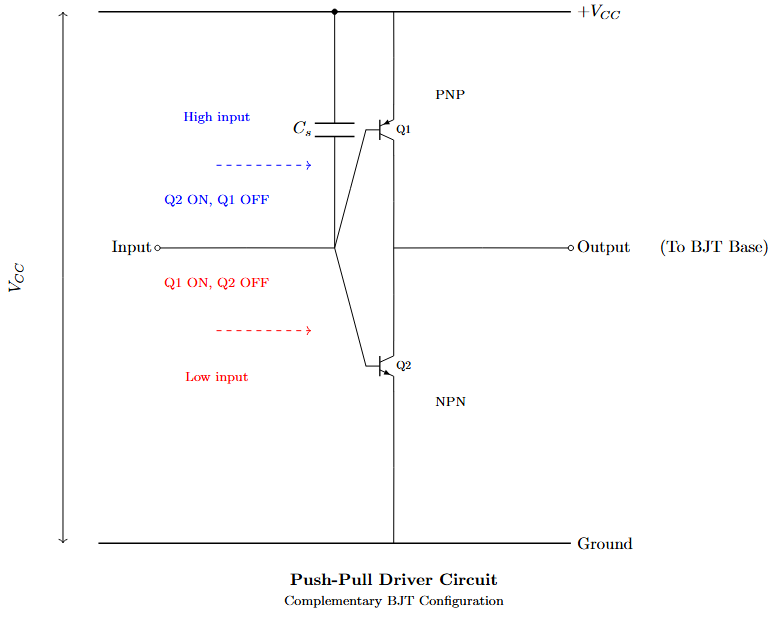
Features:
-
Fast turn-on and turn-off
-
Low output impedance
-
Positive and negative drive capability
Baker Clamp Circuit:
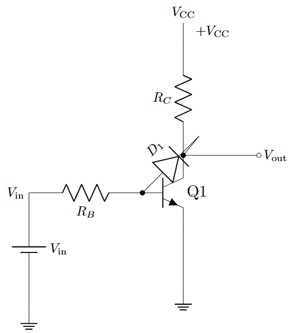
Advantages:
-
Prevents deep saturation
-
Reduces storage time
-
\(V_{BC}\) clamped to diode drop
-
Faster turn-off
Proportional Base Drive
Concept:
-
Base current proportional to collector current
-
Automatic adjustment for load variations
-
Constant overdrive factor
-
Improved efficiency
Implementation:
-
Current transformer coupling
-
Current mirror circuits
-
Feedback control systems
-
Turns ratio determines drive level
Current Transformer Drive:

Advantages:
-
Self-regulating
-
Reduced drive power
-
Isolation between control and power
Thermal Characteristics and Management
Power Dissipation:
Thermal Resistance Network:
Typical Values:
-
\(R_{\text{th}(j-c)} = 0.5 - 2 ~ \mathrm{^{\circ}CW^{-1}}\)
-
\(T_{j(\text{max})} = 150-200~\mathrm{^{\circ}C}\)
-
Derating above \(25~\mathrm{^{\circ}C}\)
Thermal Equivalent Circuit:
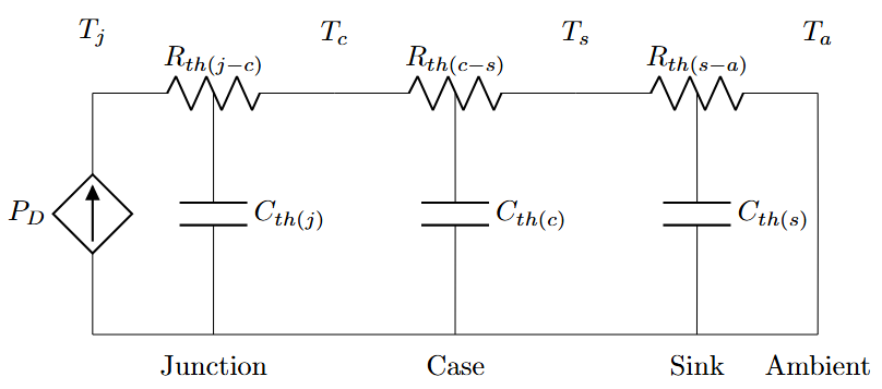
Heatsink Selection:
Thermal Protection and Derating
Protection Methods:
-
Temperature sensors (thermistors, RTDs)
-
Thermal shutdown circuits
-
Current limiting
-
Overtemperature indicators
Derating Guidelines:
-
Power derating: 2 mW °C−1–5 mW °C−1 above 25 °C
-
Current derating with temperature
-
Voltage derating at high temperatures
-
Frequency derating for switching applications
Temperature Effects:
-
\(\beta\) increases with temperature (positive temperature coefficient)
-
\(V_{BE}\) decreases at −2 mV °C −1
-
Leakage current doubles every 10 °C
-
Thermal runaway risk in parallel devices
Design Margins:
-
Use 50-70% of maximum ratings
-
Consider worst-case ambient temperature
-
Account for aging effects
-
Include safety factors for critical applications
Applications of Power BJTs
Switching Applications:
-
DC-DC converters (Buck, Boost, Buck-boost)
-
Inverters and motor drives
-
Switching power supplies
-
UPS systems
-
Welding equipment
-
High-frequency switching circuits
Linear Applications:
-
Audio power amplifiers
-
Linear regulators
-
Servo amplifiers
-
Test equipment
-
Class A/AB amplifiers
Advantages in Applications:
-
High current handling capability
-
Good linearity in active region
-
Mature technology with proven reliability
-
Cost-effective for medium power applications
-
Easy parallel operation with ballast resistors
Limitations:
-
Slower switching compared to MOSFETs
-
Requires continuous base drive current
-
Storage time limits switching frequency
-
Second breakdown susceptibility
-
Temperature-dependent characteristics
Design Example: Buck Converter Switch
Specifications:
-
Input voltage: \(V_{in} = {48}{~\mathrm{V}}\)
-
Output voltage: \(V_{out} = {12}{~\mathrm{V}}\)
-
Load current: \(I_L = {10}{~\mathrm{A}}\)
-
Switching frequency: \(f_s = 20 ~ \mathrm{kHz}\)
-
Efficiency target: \(\eta > 85\%\)
BJT Selection Criteria:
-
\(V_{CEO} \geq 1.5 \times V_{in} = {72}{~\mathrm{V}}\)
-
\(I_{C(\max)} \geq 1.5 \times I_L = {15}{~\mathrm{A}}\)
-
\(P_D\) capability for losses
-
\(\beta \geq 20\) (minimum)
-
\(t_s < {1}{\mathrm{\mu s}}\) for 20 kHz
Loss Calculations:
Base Drive Design:
Power BJT vs Other Power Devices
| Parameter | Power BJT | Power MOSFET | IGBT | Thyristor |
|---|---|---|---|---|
| Voltage Rating | 50 V–1500 V | 20 V–1000 V | 600 V–6500 V | 400 V–8000 V |
| Current Rating | 1 A–500 A | 1 A–200 A | 10 A–3000 A | 100 A–5000 A |
| Switching Speed | Slow (μs) | Fast (ns) | Medium (ns) | Very Slow (ms) |
| Drive Power | High | Low | Medium | Medium |
| Conduction Loss | Medium | Low-High | Low | Very Low |
| Switching Loss | High | Low | Medium | Low |
| Control | Current | Voltage | Voltage | Current/Voltage |
Selection Guidelines:
-
BJTs: Medium power, low frequency, cost-sensitive applications
-
MOSFETs: High frequency, low-medium power, efficiency critical
-
IGBTs: High power, medium frequency, motor drives
-
Thyristors: Very high power, low frequency, phase control
Technology Trends and Future Outlook
Current Trends:
-
Improved manufacturing processes
-
Better thermal packaging
-
Enhanced switching characteristics
-
Integration with driver circuits
-
Smart power modules
Niche Applications:
-
Audio applications (superior linearity)
-
RF power amplifiers
-
Rugged/military applications
-
Cost-sensitive consumer products
-
Replacement/maintenance applications
Challenges:
-
Competition from MOSFETs and IGBTs
-
Limited switching frequency capability
-
Base drive complexity
-
Thermal management requirements
-
Second breakdown limitations
Future Developments:
-
SiC and GaN alternatives dominating
-
Specialized applications focus
-
Improved manufacturing for cost reduction
-
Enhanced packaging technologies
-
Smart power integration
Key Takeaways
Understanding Power BJTs:
-
Current-controlled devices requiring base drive
-
Storage time dominates switching behavior
-
Thermal management is critical
-
Second breakdown limits safe operating area
-
Lower \(\beta\) compared to small-signal BJTs
Design Considerations:
-
Base drive circuit design is crucial
-
Overdrive factor for reliable saturation
-
Negative base current for fast turn-off
-
Adequate heatsinking for thermal management
-
Protection circuits for safe operation
Applications Strategy:
-
Best suited for medium power, low frequency
-
Cost-effective for specific applications
-
Linear applications benefit from good characteristics
-
Consider alternatives for high-frequency switching
-
Parallel operation possible with proper design
Design Process:
-
Define specifications and select device
-
Design base drive circuit
-
Calculate losses and thermal design
-
Implement protection circuits
-
Verify safe operating area compliance