Review: Conventional Thyristor Limitations
-
Thyristors are excellent power switches with high voltage and current ratings
-
Turn-ON: Apply positive gate current \(I_g > 0\) between gate and cathode
-
Once ON, thyristor remains conducting until anode current drops below holding current \(I_H\)
-
Natural commutation: AC supply naturally drives current to zero
-
Forced commutation: External LC circuits force current to zero
-
Cannot turn OFF using gate signal
-
Forced commutation circuits are bulky, complex, and expensive
Question: How can we overcome this limitation?
Answer: Gate Turn-Off Thyristor (GTO)
What is a GTO?
-
GTO = Gate Turn-Off Thyristor
-
A modified thyristor that can be turned OFF by applying negative gate current
-
Turn-ON: Positive gate current \(I_g > 0\) (similar to conventional thyristor)
-
Turn-OFF: Negative gate current \(I_g < 0\) of sufficient magnitude
-
Self-commutating capability eliminates need for external commutation circuits
-
DC-AC inverters (UPS systems)
-
DC choppers for motor drives
-
Variable frequency drives (VFDs)
-
High-power switching applications
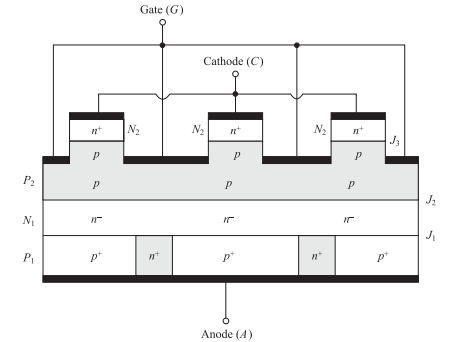
GTO Structure and Construction
-
Four-layer \(p\)-\(n\)-\(p\)-\(n\) semiconductor device
-
Three terminals: Anode (A), Cathode (K), Gate (G)
-
Highly interdigitated gate-cathode structure
-
Anode shorts: \(n^+\) regions penetrate \(p\)-type anode layer
-
Reduced \(p_1\) layer thickness for better turn-OFF
-
Shorter carrier lifetime in drift region (\(\tau = 1\,\mathrm{\mu s}\) to \(10\,\mathrm{\mu s}\))
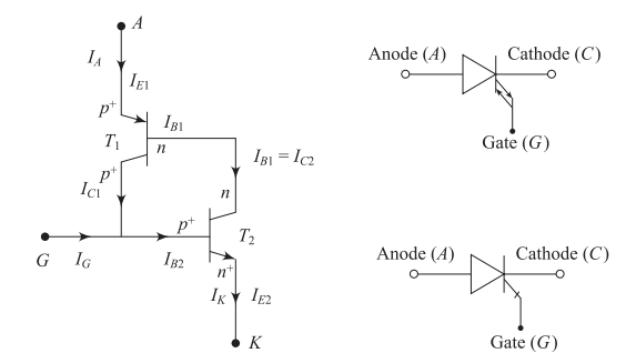
Two-Transistor Model and Circuit Symbol
-
\(T_1\): \(p\)-\(n\)-\(p\) transistor (upper)
-
\(T_2\): \(n\)-\(p\)-\(n\) transistor (lower)
-
Common base connection
-
Regenerative feedback loop
-
Similar to thyristor
-
Two-way arrow on gate indicates bidirectional control
-
Distinguishes GTO from conventional thyristor
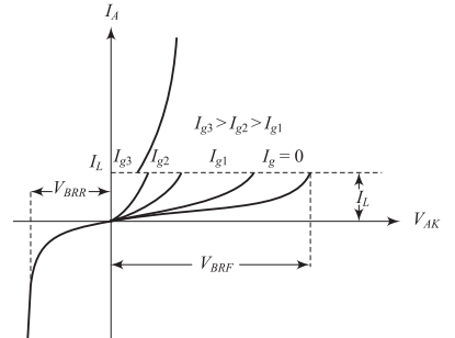
I-V Characteristics of GTO
-
Similar shape to conventional thyristor but with higher switching currents
-
Forward breakover voltage: \(V_{\mathrm{BO}} = 200\,\mathrm{V}\) to \(8000\,\mathrm{V}\)
-
Latching current: \(I_L = 2\,\mathrm{A}\) to \(10\,\mathrm{A}\)
-
Holding current: \(I_H = 200\,\mathrm{mA}\) to \(500\,\mathrm{mA}\)
-
Higher ON-state voltage drop: \(V_{\mathrm{TM}} = 2\,\mathrm{V}\) to \(4\,\mathrm{V}\)
-
Poor reverse blocking capability
-
Reverse breakdown voltage: Only \(20\,\mathrm{V}\) to \(30\,\mathrm{V}\)
-
Due to anode-short structure and heavy doping
-
Consequence: Requires anti-parallel diode for AC applications
Forward Blocking Mode
Conditions: \(V_{\mathrm{AK}} < V_{\mathrm{BO}}\) and \(I_g = 0\)
Both transistors operate with small current gains: \(\alpha_1, \alpha_2 \ll 1\)
Condition for blocking: \(\alpha_1 + \alpha_2 < 1\)
Anode current equation:
-
\(I_{\mathrm{CO1}}, I_{\mathrm{CO2}}\): Reverse saturation currents of junctions \(J_1\) and \(J_3\)
-
\(I_g\): Gate current (zero in blocking mode)
-
Since \(\alpha_1 + \alpha_2 < 1\), denominator is positive and \(I_A\) remains small
Result: GTO blocks forward voltage with only small leakage current
Turn-ON Process
-
Apply positive gate current: \(I_g > I_{\mathrm{gt}}\) (gate trigger current)
-
Gate current increases base current of transistor \(T_2\)
-
\(T_2\) starts conducting, increasing its collector current
-
Collector current of \(T_2\) becomes base current of \(T_1\)
-
\(T_1\) starts conducting, providing base current to \(T_2\)
-
Regenerative action: Both transistors saturate rapidly
-
Minimum gate current: \(I_{\mathrm{gt}} = 0.1\,\mathrm{A}\) to \(1\,\mathrm{A}\)
-
Gate trigger voltage: \(V_{\mathrm{gt}} = 2\,\mathrm{V}\) to \(5\,\mathrm{V}\)
Turn-OFF Process
-
Apply negative gate voltage: \(V_{\mathrm{gk}} < 0\)
-
Negative gate current extracts holes from \(p_1\) base region
-
Base current of transistor \(T_2\) becomes negative
-
\(T_2\) exits saturation and current gain drops
-
Junction \(J_2\) becomes reverse biased
-
Electron injection from cathode stops
-
Stored charge recombines, causing tail current
-
GTO regains forward blocking capability
For transistor \(T_2\) to exit saturation:
Turn-ON Characteristics
-
Peak gate current: \(I_{\mathrm{gp}} = 10\%\) to \(50\%\) of anode current
-
Rate of rise: \(\frac{\mathrm{d}i_g}{\mathrm{d}t} > 10\,\mathrm{A/\mu s}\)
-
Pulse width: \(t_g = 10\,\mathrm{\mu s}\) to \(50\,\mathrm{\mu s}\)
-
Back-porch current: Small current maintained during ON-state
-
Delay time: \(t_d = 0.5\,\mathrm{\mu s}\) to \(2\,\mathrm{\mu s}\)
-
Rise time: \(t_r = 1\,\mathrm{\mu s}\) to \(5\,\mathrm{\mu s}\)
-
Total turn-ON time: \(t_{\mathrm{on}} = t_d + t_r\)
-
All cathode segments must turn ON simultaneously
-
High \(\frac{\mathrm{d}i_g}{\mathrm{d}t}\) prevents current crowding
-
Low gate circuit inductance essential
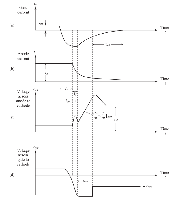
Turn-OFF Characteristics
-
Peak reverse current: \(|I_g| = \frac{I_A}{\beta_{\mathrm{off}}}\)
-
Rate of fall: \(\left|\frac{\mathrm{d}i_g}{\mathrm{d}t}\right| > 100\,\mathrm{A/\mu s}\)
-
Gate resistance: \(R_g < 1\,\mathrm{\Omega}\) for fast turn-OFF
-
Storage time: \(t_s = 5\,\mathrm{\mu s}\) to \(50\,\mathrm{\mu s}\)
-
Fall time: \(t_f = 5\,\mathrm{\mu s}\) to \(20\,\mathrm{\mu s}\)
-
Tail time: \(t_{\mathrm{tail}} = 50\,\mathrm{\mu s}\) to \(500\,\mathrm{\mu s}\)
-
Total: \(t_{\mathrm{off}} = t_s + t_f + t_{\mathrm{tail}}\)
Key GTO Ratings
-
\(V_{\mathrm{DRM}}\): Peak repetitive forward blocking voltage
( \(1200\,\mathrm{V}\) to \(6000\,\mathrm{V}\)) -
\(V_{\mathrm{RRM}}\): Peak repetitive reverse voltage
( \(20\,\mathrm{V}\) to \(30\,\mathrm{V}\)) -
\(V_{\mathrm{TM}}\): Peak on-state voltage
( \(2\,\mathrm{V}\) to \(4\,\mathrm{V}\))
-
\(I_{\mathrm{T(RMS)}}\): RMS on-state current
( \(50\,\mathrm{A}\) to \(6000\,\mathrm{A}\)) -
\(I_H\): Holding current
( \(200\,\mathrm{mA}\) to \(500\,\mathrm{mA}\)) -
\(I_L\): Latching current
( \(2\,\mathrm{A}\) to \(10\,\mathrm{A}\))
-
Turn-OFF gain: \(\beta_{\mathrm{off}} = 3\) to \(10\)
-
Maximum switching frequency: Up to \(10\,\mathrm{kHz}\)
-
\(\frac{\mathrm{d}i}{\mathrm{d}t}\) capability : \(100\,\mathrm{A/\mu s}\) to \(1000\,\mathrm{A/\mu s}\)
-
Junction temperature: Up to \(125\,\mathrm{^\circ C}\)
-
Thermal resistance: \(0.1\,\mathrm{K/W}\) to \(1\,\mathrm{K/W}\)
-
Power dissipation: Critical for high-frequency operation
GTO vs Conventional Thyristor
| GTO | Conventional Thyristor |
|---|---|
| Self turn-OFF capability | Requires external commutation |
| Higher latching current (\(2\,\mathrm{A}\) to \(10\,\mathrm{A}\)) | Lower latching current (\(50\,\mathrm{mA}\) to \(500\,\mathrm{mA}\)) |
| Higher ON-state drop (\(2\,\mathrm{V}\) to \(4\,\mathrm{V}\)) | Lower ON-state drop (\(1\,\mathrm{V}\) to \(2\,\mathrm{V}\)) |
| Complex gate drive circuits | Simple gate drive |
| Poor reverse blocking (\(20\,\mathrm{V}\) to \(30\,\mathrm{V}\)) | Good reverse blocking (same as forward) |
| Faster switching (up to \(10\,\mathrm{kHz}\)) | Slower switching (up to \(1\,\mathrm{kHz}\)) |
| Compact circuit size | Bulky commutation circuits |
| Higher gate drive losses | Lower gate drive losses |
GTO Protection Requirements
-
High \(\frac{\mathrm{d}v}{\mathrm{d}t}\) during turn-OFF can cause false turn-ON
-
High \(\frac{\mathrm{d}i}{\mathrm{d}t}\) during turn-ON can damage the device
-
Gate-cathode junction needs protection from overvoltage
-
Turn-OFF snubber (RC circuit across anode-cathode):
-
Limits \(\frac{\mathrm{d}v}{\mathrm{d}t}\) during turn-OFF
-
Typical values: \(R = 10\,\mathrm{\Omega}\) to \(100\,\mathrm{\Omega}\), \(C = 0.1\,\mathrm{\mu F}\) to \(10\,\mathrm{\mu F}\)
-
-
Turn-ON snubber (series inductor):
-
Limits \(\frac{\mathrm{d}i}{\mathrm{d}t}\) during turn-ON
-
-
Gate protection: Zener diodes across gate-cathode
-
Overcurrent protection: Fast-acting fuses
-
Adequate heat sinking required due to higher conduction losses
-
Junction temperature monitoring essential
Advantages and Disadvantages of GTO
-
Self turn-OFF capability
-
Eliminates commutation circuits
-
Faster switching than SCRs
-
Higher power density
-
Reduced electromagnetic interference
-
Simplified control circuits
-
Better dynamic response
-
Complex gate drive circuits
-
Higher gate drive power
-
Poor reverse blocking
-
Higher conduction losses
-
Limited switching frequency
-
Requires anti-parallel diode
-
More expensive than SCRs
Trade-off: Higher complexity and cost vs. improved performance and circuit simplification
Applications of GTO
1. Variable Speed Drives:
-
DC motor drives (choppers)
-
AC motor drives (voltage source inverters)
-
High-performance industrial drives
2. Power System Applications:
-
Static VAR compensators (SVCs)
-
High-voltage DC transmission (HVDC)
-
Power quality improvement systems
3. Traction Systems:
-
Railway locomotive drives
-
Electric vehicle propulsion
4. Industrial Applications:
-
Uninterruptible power supplies (UPS)
-
Induction heating
-
Welding equipment
Summary and Key Points
-
GTO provides controllable turn-OFF capability through negative gate current
-
Structural modifications enable turn-OFF: anode shorts, interdigitated structure
-
Turn-OFF gain \(\beta_{\mathrm{off}} = I_A/|I_g|\) is typically 3–10
-
Trade-offs: Better controllability vs. higher complexity and losses
-
Requires protection circuits and anti-parallel diode
-
Gate drive circuit design is critical
-
Snubber circuits are mandatory
-
Thermal management is important
-
Consider switching frequency limitations
-
GTOs paved the way for modern self-commutated devices
-
Being replaced by IGBTs and IGCTs in many applications
-
Still used in very high power applications (\(1\,\mathrm{MW}\) and above)