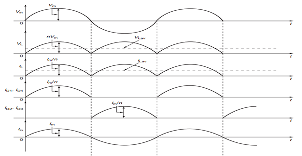
Single-Phase Full-Wave Diode Rectifier:
Bridge Rectifier:
Lower peak diode voltage.
Suitable for high-voltage applications.
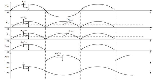
Center-Tapped Transformer Rectifier:
Provides electrical isolation.
Only one diode voltage drop between source and load.
Desirable for low-voltage, high-current applications.
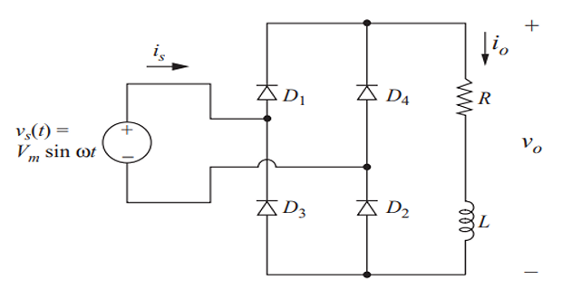
Full-Wave Bridge Rectifier:
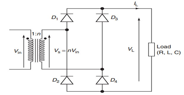
Diode Conducting Pairs:
D1 & D2 conduct together.
D3 & D4 conduct together.
Kirchhoff’s Voltage Law (KVL):
D1 & D3 cannot be on simultaneously.
D2 & D4 cannot conduct simultaneously.
Load Current:
Positive or zero.
Never negative.
Load Voltage:
+\(v_s\) when D1 & D2 are on.
+\(v_s\) when D3 & D4 are on.
Reverse-Biased Diode Voltage:
Maximum is the peak value of the source.
With D1 on, the voltage across D3 is -\(v_s\).
Source Current:
Current entering the bridge: \(i_{D1} - i_{D4}\).
Symmetric about zero.
Average source current: zero.
RMS source current = RMS load current.
Source current = load current for half the period.
Source current = -load current for the other half.
Squares of load and source currents are equal, so RMS currents are equal.
Output Voltage Frequency:
Fundamental frequency: \(2\omega\) (twice the AC input frequency).
Output Voltage Fourier Series:
Consists of a DC term and even harmonics of the source frequency.
The Center-Tapped Transformer Rectifier
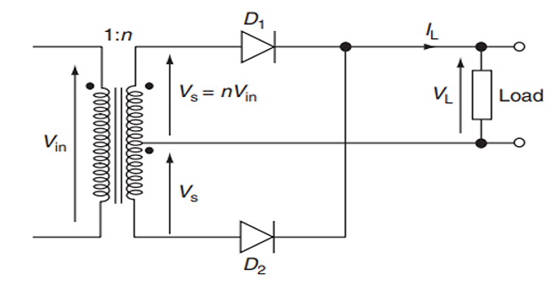
Kirchhoff’s Voltage Law (KVL):
Only one diode can conduct at a time.
Load Current:
Positive or zero.
Never negative.
Output Voltage:
+\(v_{s1}\) when D1 conducts.
-\(v_{s2}\) when D2 conducts.
Transformer Secondary Voltages:
Related to the source voltage by \(v_{s1} = v_{s2} = v_s \left(\frac{N_2}{2N_1}\right)\).
Reverse-Biased Diode Voltage:
Maximum is twice the peak value of the load voltage.
Shown by KVL around the transformer secondary windings, D1, and D2.
Source Current:
Current in each half of the transformer secondary is reflected to the primary.
Average source current: zero.
Transformer Function:
Provides electrical isolation between the source and the load.
Output Voltage Frequency:
Fundamental frequency: \(2\omega\) (twice the AC input frequency).
Resistive Load
- The voltage across a resistive load\[\nu_o(\omega t)=\begin{cases}V_m\sin\omega t&\quad\mathrm{for~}0\leq\omega t\leq\pi\\-V_m\sin\omega t&\quad\mathrm{for~}\pi\leq\omega t\leq2\pi\end{cases}\]
- The dc component of the output voltage is the average value, and load current is simply the resistor voltage divided by resistance\[\begin{aligned} V_o&=\frac{1}{\pi}\int\limits_0^\pi V_m\sin\omega td(\omega t)=\frac{2V_m}{\pi}\\ I_o & =\frac{V_o}{R}=\frac{2V_m}{\pi R} \end{aligned}\]
Power absorbed by the load resistor \(= I_{\mathrm{rms}}^2 \cdot R\), where \(I_{\mathrm{rms}} = \dfrac{I_m}{\sqrt{2}}\)
Power factor \(= 1\)
RL-Load
Load Current (\(i_o\)):
Reaches a periodic steady-state condition after a start-up transient.
Full-Wave Rectified Sinusoidal Voltage Across the Load:
Can be expressed as a Fourier series.
Consists of a DC term and the even harmonics.
\[\begin{aligned} \nu_o(t) & =V_o+\sum_{n=2,4\ldots}^\infty V_n\cos{(n\omega_0t+\pi)}\\ V_o & =\frac{2V_m}{\pi}\quad\text{and}\quad V_n=\frac{2V_m}{\pi}\left(\frac{1}{n-1}-\frac{1}{n+1}\right) \end{aligned}\]
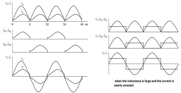
Current in the RL Load:
Computed using superposition.
Each frequency is considered separately and results are combined.
DC Current and Current Amplitude:
- Computed for each frequency.\[\begin{aligned} I_0 & =\frac{V_0}{R} \quad ~\text{and}~\quad I_n & =\frac{V_n}{Z_n}=\frac{V_n}{|R+jn\omega L|} \end{aligned}\]
- (load inductance may be relatively large or made large by adding external inductance) If\[i(\omega t)\approx I_o=\frac{V_o}{R}=\frac{2V_m}{\pi R}\quad ~\text{and}~ \quad~ I_{\mathrm{rms}}\approx I_o\]
Harmonic (\(n\)) Effects:
\(n~\uparrow~\Rightarrow~V_n~\downarrow\).
For an RL load, as \(n~\uparrow ~\Rightarrow ~Z_n~\uparrow\).
Combination of \(V_n~\downarrow ~ + ~Z_n~\uparrow~\Rightarrow ~I_n~\downarrow\) rapidly with \(n~\uparrow\).
Significance in RL Load:
DC term and only a few AC terms are usually necessary to describe the current in an RL load.
RLE-Load
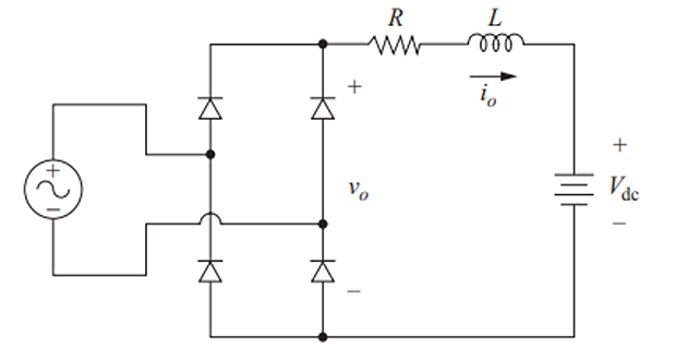
Applications:
DC motor drive circuit.
Battery charger.
Modes of Operation:
Continuous-current mode.
Discontinuous-current mode.
- The dc (average) component of current in this circuit:\[\boxed{I_o=\frac{V_o-V_{\mathrm{dc}}}{R}=\frac{\frac{2V_m}{\pi}-V_{\mathrm{dc}}}{R}}\]
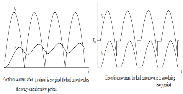
Continuous-Current Mode:
Load current is always positive for steady-state operation.
One pair of diodes is always conducting.
Voltage across the load is a full-wave rectified sine wave.
Only modification to the RL load analysis is in the DC term of the Fourier series.
Discontinuous-Current Mode:
Load current returns to zero during every period.
Capacitance Output Filter
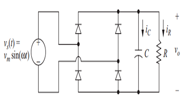
Produces an output voltage that is essentially DC.
Analysis similar to that of the half-wave rectifier with a capacitance filter.
Capacitor discharge time is smaller than in the half-wave circuit due to the rectified sine wave in the second half of each period.
Output voltage ripple for the full-wave rectifier is approximately half that of the half-wave rectifier.
Peak output voltage is less in the full-wave circuit due to two diode voltage drops rather than one.
Output voltage is a positive sine function when one of the diode pairs is conducting.
Output voltage is a decaying exponential otherwise.
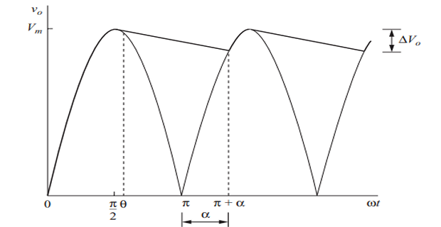
- Assuming ideal diodes,\[\nu_o(\omega t)=\begin{cases}\left|V_m\sin\omega t\right|&\text{one diode pair on}\\(V_m\sin\theta)e^{-(\omega t-0)/\omega RC}&\text{diodes off}\end{cases}\]
The diodes become reverse biased at \(\theta\)
\[\theta=\tan^{-1}(-\omega RC)=-\tan^{-1}(\omega RC)+\pi\]The maximum output voltage (\(V_m\)) , and the minimum output voltage is determined by evaluating \(\nu_o\) at the angle at which the second pair of diodes turns on, which is at \(\omega t = \pi + \alpha\). At that boundary point
\[\begin{aligned} & (V_m\sin\theta)e^{-(\pi+\alpha-\theta)/\omega RC}=-V_m\sin\left(\pi+\alpha\right) \\ \Rightarrow &~(\sin\theta)e^{-(\pi+\alpha-\theta)/\omega RC}-\sin\alpha=0\\ & \text{Solve numerically for}~\alpha \end{aligned}\]
- The peak-to-peak voltage variation, or ripple, is the difference between maximum and minimum voltages\[\boxed{\Delta V_o=V_m-\begin{vmatrix}V_m\sin{(\pi+\alpha)}\end{vmatrix}=V_m(1-\sin{\alpha})}\]
\(\alpha\) is larger for the full-wave rectifier and the ripple is smaller for a given load
The peak-to-peak ripple
\[\boxed{\Delta V_o\approx\frac{V_m\pi}{\omega RC}=\frac{V_m}{2fRC}}\]Note that the approximate peak-to-peak ripple voltage for the full-wave rectifier is one-half that of the half-wave rectifier