Introduction
This experiment converts single-phase AC to DC using a full-wave bridge diode rectifier. The circuit is implemented in MATLAB Simulink and verified with a hardware prototype. Both resistive and RL loads are studied.
Determine RMS, average, form factor, and ripple factor for R and RL loads. Perform FFT harmonic analysis and compare simulation vs hardware measurements.
Theory
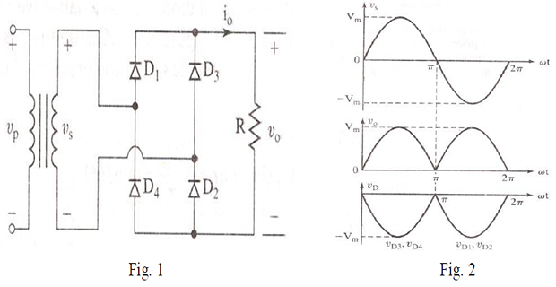
A full-wave bridge rectifier uses four diodes (D1–D4). During the positive half-cycle, D1 and D2 conduct; during the negative half-cycle, D3 and D4 conduct. For a resistive load, the output current tracks the output voltage waveform.
Simulation — R Load (Problem 1)
Implement the 1-phase uncontrolled full-wave rectifier with R = 25 Ω. Input: \(V_{peak} = 50\text{ V}\) (35.35 V RMS), 50 Hz. Attach waveforms and perform FFT analysis.

Simulation — RL Load (Problem 2)
Add L = 6 mH in series with R = 25 Ω. Observe changes in output voltage waveform and FFT analysis. Compare with pure R load results.
Hardware — R Load
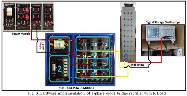
- Connect circuit as in Fig. 3 (R = 25 Ω). Switch ON 3φ supply MCB.
- Switch ON POWER MODULE MCB and SCR–Diode Power Module MCB.
- Increase voltage slowly to 35.35 V RMS using + push button.
- Connect CRO probes across R load. Observe output voltage waveforms and FFT in DSO.
Hardware — RL Load
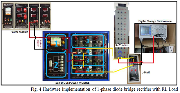
- Connect circuit as in Fig. 4 (R = 25 Ω, L = 6 mH). Switch ON 3φ supply MCB.
- Repeat the hardware procedure from the R-load section (steps 2–4).
Results
Required waveforms to attach (Simulink & Hardware): Output Voltage, Output Current, Diode Voltage, Diode Current, Input Voltage, Input Current, FFT bar charts.
Performance Parameters — Simulation
| Parameter | R Load | RL Load |
|---|---|---|
| VRMS (V) | ||
| IRMS (A) | ||
| VAVG (V) | ||
| IAVG (A) | ||
| Form Factor | ||
| Ripple Factor |
Performance Parameters — Hardware
| Parameter | R Load | RL Load |
|---|---|---|
| VRMS (V) | ||
| VAVG (V) | ||
| Form Factor | ||
| Ripple Factor |
FFT Analysis
| Parameter | R Load — Sim | R Load — HW | RL Load — Sim | RL Load — HW |
|---|---|---|---|---|
| THD (%) | ||||
| Vfundamental (RMS) | ||||
| V 2nd Harmonic (RMS) | ||||
| V 3rd Harmonic (RMS) | ||||
| ITHD (%) | ||||
| Ifundamental (RMS) | ||||
| I 2nd Harmonic (RMS) | ||||
| I 3rd Harmonic (RMS) |