Introduction & Theory
A power inverter converts DC to AC. The single-phase full-bridge Voltage Source Inverter (VSI) uses four switches (IGBTs/MOSFETs) to produce an AC waveform from a DC source. The output voltage waveform shape and harmonic content depend on the modulation strategy.
Input is a stiff DC voltage source. Directly controls AC output voltage. Uses feedback diodes to allow current flow when switches are OFF (essential for RL loads).
Input is a current source. Directly controls AC output current. Less common in modern low-voltage applications.
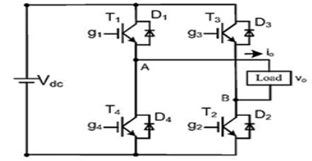
Feedback (freewheeling) diodes are essential for RL loads because the output current Io is not in phase with voltage Vo. When a switch turns OFF, the inductor drives current through the corresponding feedback diode back to the DC source.
Square wave produces high THD (~48%) but simple gate drive. Unipolar PWM with sinusoidal reference reduces THD significantly. Higher modulation index (MI) ⇒ larger fundamental output voltage.
Square Wave Modulation
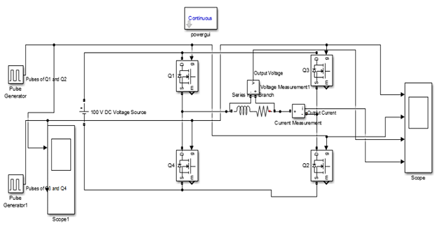
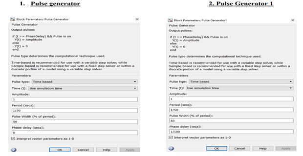
R = 12.5 Ω, L = 6 mH, Vdc = 100 V. Switches S1&S4 ON for first half-cycle, S2&S3 ON for second half-cycle. Output = ±100 V square wave at 50 Hz.
Unipolar PWM Modulation
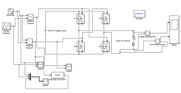
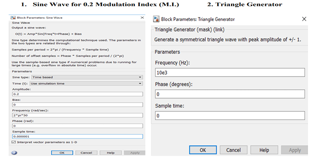
Same RL load and Vdc. Sinusoidal reference (50 Hz) compared with high-frequency triangular carrier to generate gate pulses. Test MI = 1.0, 0.6, and 0.2.
Observation Table
| S.No | Input Voltage / Mode | Vo,fund RMS (V) | Vo,THD (%) | Vo RMS at 150 Hz (V) | Io,fund RMS (A) | Io RMS at 150 Hz (A) | Io,THD (%) |
|---|---|---|---|---|---|---|---|
| 1 | Square Wave — 100 V | ||||||
| 2 | Unipolar PWM, MI = 1.0, 100 V | ||||||
| 3 | Unipolar PWM, MI = 0.6, 100 V | ||||||
| 4 | Unipolar PWM, MI = 0.2, 100 V |
Results
I. Square Wave Modulation
- Attach the MATLAB Simulink circuit diagram of square wave modulation inverter.
- Attach waveforms: (a) Output Voltage (b) Output Current
- Attach the FFT plot of output voltage and output current. Record THD, Vfundamental, 3rd harmonic, 5th harmonic.
II. Unipolar PWM Modulation (MI = 0.2)
- Attach the MATLAB Simulink circuit diagram of unipolar PWM inverter.
- Attach waveforms at MI = 0.2: (a) Output Voltage (b) Output Current
- Attach FFT plots at MI = 0.2. Compare THD with square wave case.
Square wave THD ≈ 48%. Unipolar PWM (MI = 1.0) achieves THD below 5% for the output current due to the RL load filtering action. This justifies the additional complexity of PWM control.