Introduction
This experiment introduces Power Electronics circuit simulation using MATLAB Simulink. A half-wave diode rectifier is simulated and the results are verified experimentally. The laboratory bridges theoretical knowledge with practical measurement techniques using industry-standard tools.
Learning Outcomes
Build and simulate power electronic circuits using the Simscape Specialized Power Systems library.
Extract DC average, RMS values, harmonic content, and THD using the Powergui FFT Analysis tool.
Implement the circuit in hardware using the Power Module kit and compare with DSO measurements.
Familiarization with MATLAB / Simulink
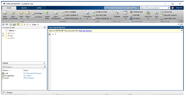
- Launch MATLAB and click New → Simulink Model. Save the new
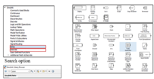
.slxfile. - Open the Simulink Library Browser from the toolbar.
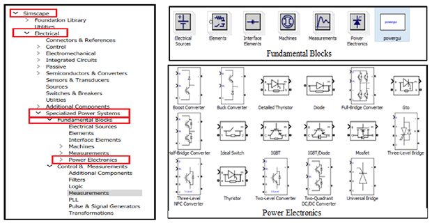
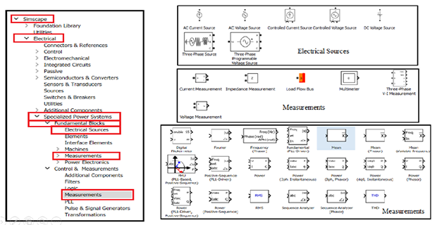
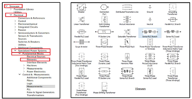
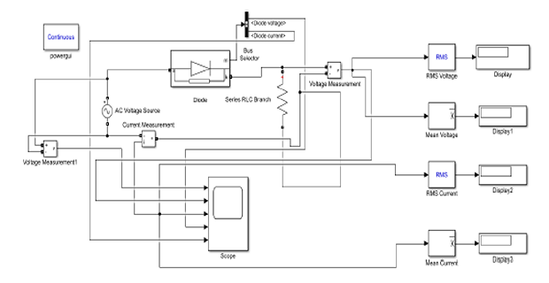
- Navigate to Simscape → Electrical → Specialized Power Systems → Fundamental Blocks → Power Electronics.
- Drag and connect components. Use Voltage/Current Measurement blocks and a Scope.
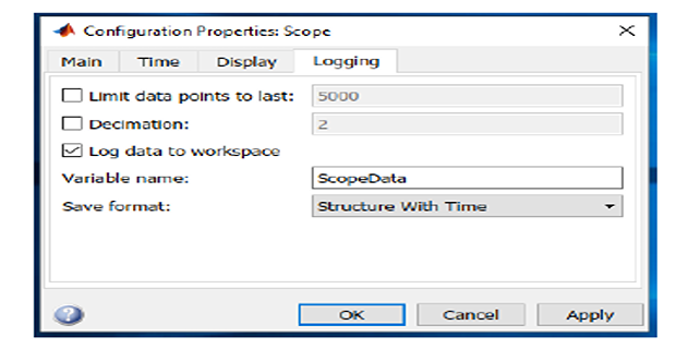
- Add a Powergui block (required). Configure scope logging: enable Log data to workspace (Structure with time).
.slx file.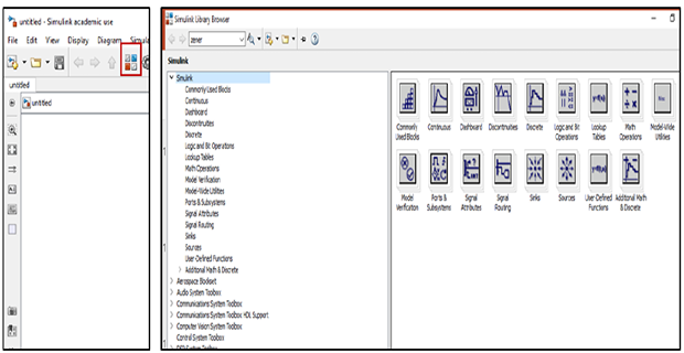
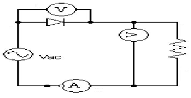
Problem 1 — Half-Wave Rectifier with R Load
Implement a 1-phase half-wave diode rectifier with R = 100 Ω. Input: \(V_{peak} = 50\text{ V}\) (35.35 V RMS), 50 Hz. Observe waveforms and perform FFT analysis.
Key formulas:
- \(V_{dc} = V_m/\pi\)
- \(V_{rms} = V_m/2\)
- Form Factor \(= V_{rms}/V_{dc} = \pi/2 \approx 1.571\)
Simulink procedure:
- Run simulation for 0.5 s
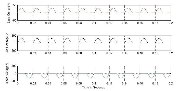
- Observe waveforms in Scope
- Use Powergui FFT for harmonic analysis
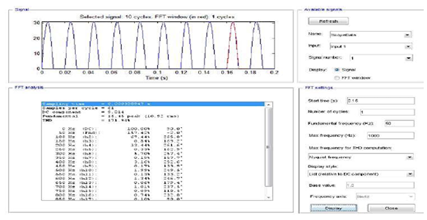
FFT Analysis using Powergui
- Double-click Powergui → select FFT Analysis.
- Select the workspace variable and the signal to analyse.
- Set Fundamental frequency = 50 Hz; choose Bar or List display.
- Record Vfundamental, THD, 2nd and 3rd harmonic values.

Problem 2 — Half-Wave Rectifier with RL Load
Repeat with R = 100 Ω, L = 6 mH. Observe the effect of inductance: extended conduction angle and smoother current waveform.
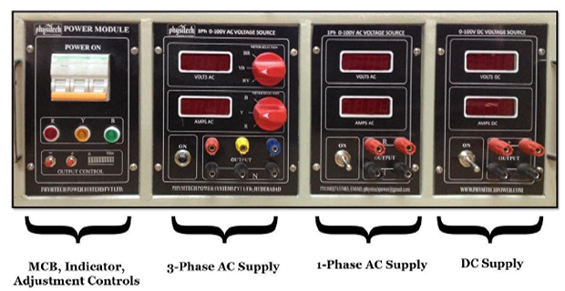
Hardware Implementation
Variable AC supply with push-button voltage adjustment. Set to 35.35 V RMS. MCB must be ON before voltage adjustments show on display.
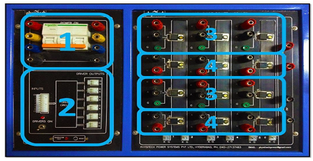
Houses all power semiconductor devices: MCB, firing signal I/O, thyristors, and diodes. Connected via banana-plug terminals.
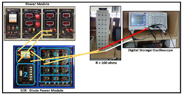
Procedure (R Load)
- Connect circuit as in Fig. 16 (R = 100 Ω). Switch ON the 3φ supply MCB.
- Switch ON POWER MODULE MCB, then SCR–Diode Power Module MCB.
- Slowly increase voltage to 35.35 V RMS using + push button.
- Connect CRO probes across R load. Observe waveforms and FFT in DSO; save to USB.
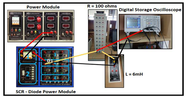
Procedure (RL Load)
- Replace R load with RL load: R = 100 Ω, L = 6 mH (Fig. 17).
- Repeat steps 2–4 above. Note the difference in waveform due to inductance.
Results
Attach waveforms: (a) Output Voltage (b) Output Current (c) Diode Voltage (d) Diode Current (e) Input Voltage — in Simulink and experimentally.
Performance Parameters — R & RL Load (Simulink)
| Parameter | R Load — Theory | R Load — Simulation | R Load — Hardware | RL Load — Theory | RL Load — Simulation |
|---|---|---|---|---|---|
| VRMS (V) | |||||
| IRMS (A) | |||||
| VAVG (V) | |||||
| IAVG (A) | |||||
| Form Factor | |||||
| Ripple Factor | |||||
| PIV (V) |
FFT Analysis
| Parameter | R Load — Sim | R Load — HW | RL Load — Sim |
|---|---|---|---|
| Vfundamental (RMS) | |||
| VTHD (%) | |||
| V 2nd Harmonic | |||
| V 3rd Harmonic | |||
| Ifundamental (RMS) | |||
| ITHD (%) | |||
| I 2nd Harmonic | |||
| I 3rd Harmonic |