0-Mark Questions
QQuestion 1 0 Mark
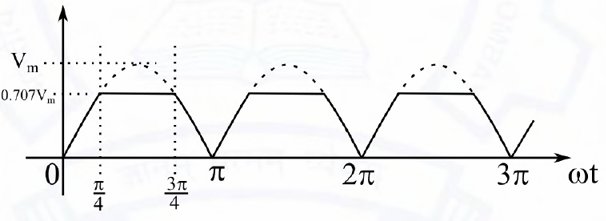
The waveform shown in solid line is obtained by clipping a full-wave rectified sinusoid (shown dashed). The ratio of the RMS value of the full-wave rectified waveform to the RMS value of the clipped waveform is \_\_\_\_\_\_\_\_. (Round off to 2 decimal places.)
SSolution
Given:
- Full-wave rectified sinusoid (dashed): \(v(t) = V_m|\sin(\omega t)|\)
- Clipped waveform (solid): Flat-topped at \(0.707V_m\) from \(\omega t = \pi/4\) to \(3\pi/4\)
- Find: Ratio of RMS values = \(\frac{V_{rms,full}}{V_{rms,clipped}}\)
Solution:
Step 1: RMS value of full-wave rectified sinusoid
For a full-wave rectified sinusoid over one complete cycle:
Using the identity \(\sin^2(x) = \frac{1 - \cos(2x)}{2}\):
Therefore:
Step 2: RMS value of clipped waveform
The clipped waveform has three regions in the half-cycle \([0, \pi]\):
- Region 1: \([0, \pi/4]\) - Rising sinusoid: \(v = V_m\sin(\omega t)\)
- Region 2: \([\pi/4, 3\pi/4]\) - Flat top: \(v = 0.707V_m\)
- Region 3: \([3\pi/4, \pi]\) - Falling sinusoid: \(v = V_m\sin(\omega t)\)
Region 1 \& 3 (by symmetry):
Both regions contribute: \(2\left(\frac{\pi}{8} - \frac{1}{4}\right) = \frac{\pi}{4} - \frac{1}{2}\)
Region 2:
Total:
Step 3: Calculate the ratio
Verification:
QQuestion 2 0 Mark
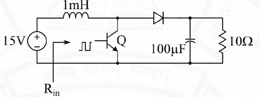
Consider the boost converter shown. Switch Q is operating at 25 kHz with a duty cycle of 0.6. Assume the diode and switch to be ideal. Under steady-state condition, the average resistance \(R_{in}\) as seen by the source is \_\_\_\_\_\_\_\_ \(\Omega\). (Round off to 2 decimal places.)
SSolution
Given:
- Input voltage: \(V_s = 15\) V
- Inductance: \(L = 1\) mH
- Capacitance: \(C = 100\) μF
- Load resistance: \(R = 10\) \(\Omega\)
- Switching frequency: \(f = 25\) kHz
- Duty cycle: \(D = 0.6\)
- Ideal switch and diode
- Find: Average input resistance \(R_{in}\)
Solution:
Step 1: Output voltage of boost converter
For a boost converter in continuous conduction mode (CCM):
Step 2: Output current
Step 3: Average input current
For an ideal boost converter, power in equals power out:
Alternatively, using the relationship:
Step 4: Input resistance
The average input resistance as seen by the source:
Alternative approach using converter relationships:
For a boost converter:
Verification:
Check power balance:
- Input power: \(P_{in} = V_s \times I_{in} = 15 \times 9.375 = 140.625\) W
- Output power: \(P_{out} = \frac{V_o^2}{R} = \frac{37.5^2}{10} = \frac{1406.25}{10} = 140.625\) W ✓
Check resistance:
QQuestion 3 0 Mark
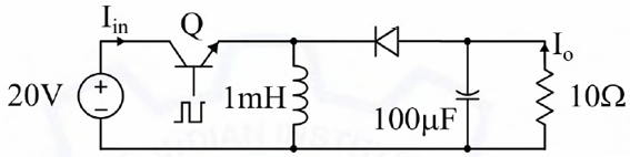
Consider the buck-boost converter shown. Switch Q is operating at 25 kHz and 0.75 duty-cycle. Assume diode and switch to be ideal. Under steady-state condition, the average current flowing through the inductor is \_\_\_\_\_\_\_\_ A. (Round off to 2 decimal places.)
SSolution
Given:
- Input voltage: \(V_{in} = 20\) V
- Inductance: \(L = 1\) mH
- Capacitance: \(C = 100\) μF
- Load resistance: \(R = 10\) \(\Omega\)
- Switching frequency: \(f = 25\) kHz
- Duty cycle: \(D = 0.75\)
- Ideal switch and diode
- Find: Average inductor current \(I_L\)
Solution:
Step 1: Output voltage of buck-boost converter
For a buck-boost converter in continuous conduction mode:
Note: The output voltage is negative with respect to ground in an inverting buck-boost, but we use magnitude for calculations.
Step 2: Output current
Step 3: Average inductor current
In a buck-boost converter, the inductor current relationship is:
During ON state (\(DT\)): Inductor connected to input, charges During OFF state (\((1-D)T\)): Inductor discharges through diode to output
The average inductor current can be found using:
Alternative verification using power balance:
For ideal converter:
Average input current:
Power balance:
Step 4: Verification using current relationships
In buck-boost converter:
- When switch ON: \(I_L\) flows from source through switch
- When switch OFF: \(I_L\) flows through diode to load
- Average input current: \(\langle I_{in} \rangle = D \times I_L\)
- Average output current: \(\langle I_o \rangle = (1-D) \times I_L\)
Check:
QQuestion 4 0 Mark
A single-phase full-bridge inverter fed by a 325 V DC produces a symmetric quasi-square waveform across 'ab' as shown. To achieve a modulation index of 0.8, the angle \(\theta\) expressed in degrees should be \_\_\_\_\_\_\_\_. (Round off to 2 decimal places.)
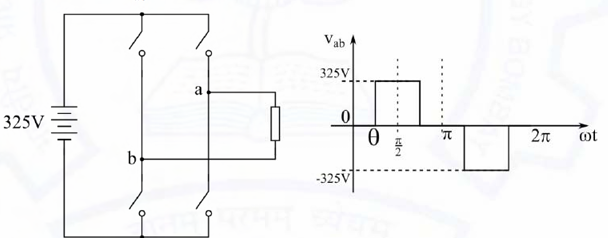
(Modulation index is defined as the ratio of the peak of the fundamental component of \(v_{ab}\) to the applied DC value.)
SSolution
Given:
- DC supply voltage: \(V_{dc} = 325\) V
- Output waveform: Symmetric quasi-square wave
- Modulation index: \(m_a = 0.8\)
- Find: Angle \(\theta\) in degrees
- Definition: \(m_a = \frac{V_1}{V_{dc}}\) where \(V_1\) is peak of fundamental
Solution:
Step 1: Understand the waveform
The quasi-square waveform has:
- \(v_{ab} = +325\) V for \(\theta < \omega t < \pi - \theta\)
- \(v_{ab} = 0\) V for \(0 < \omega t < \theta\) and \(\pi - \theta < \omega t < \pi\)
- \(v_{ab} = -325\) V for \(\pi + \theta < \omega t < 2\pi - \theta\)
- \(v_{ab} = 0\) V for \(\pi < \omega t < \pi + \theta\) and \(2\pi - \theta < \omega t < 2\pi\)
Step 2: Fourier analysis for fundamental component
For a symmetric quasi-square wave with angle \(\theta\), the fundamental component is:
This is the peak value of the fundamental component.
Derivation (Fourier series):
For \(n = 1\) (fundamental):
Step 3: Apply modulation index definition
Step 4: Calculate angle
Verification:
Check:
Modulation index: