1-Mark Questions
QQuestion 1 1 Mark
A three-phase current source inverter used for the speed control of an induction motor is to be realized using MOSFET switches as shown below. Switches \(S_1\) to \(S_6\) are identical switches. The proper configuration for realizing switches \(S_1\) to \(S_6\) is
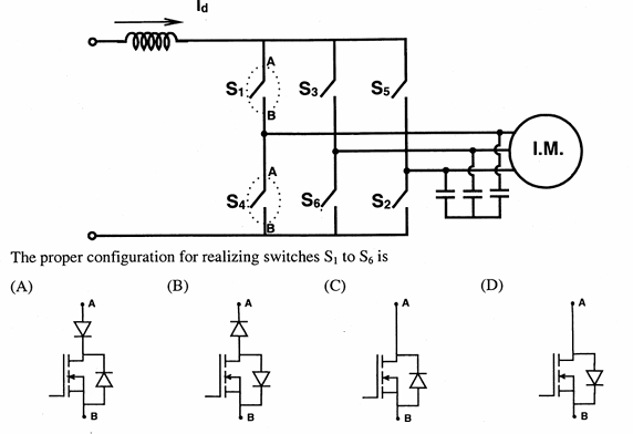
AOptions
- MOSFET only
- MOSFET with anti-parallel diode
- MOSFET with series diode (blocking reverse voltage)
- MOSFET with reverse-blocking capability
SSolution
Current Source Inverter (CSI) requirements:
Key characteristics:
- DC current source input (constant current)
- Load is induction motor (inductive)
- Switches must handle bidirectional voltage
- Switches carry unidirectional current
Why series diode is needed:
1. Reverse voltage blocking:
- During commutation, load voltage can reverse
- MOSFET body diode would conduct in reverse
- Series diode blocks reverse voltage
- Prevents short circuit through body diode
2. Current commutation:
- Current source must have continuous path
- Series diode ensures current flows only forward through MOSFET
- Prevents circulating currents
3. Configuration:
\begin{tikzpicture} \draw (0,0) to[short] (0,2); \draw (0,1) node[nigfete, anchor=D] (mosfet) {}; \draw (mosfet.S) to[diode] (0,0); \node at (0.8,1) {Series}; \node at (0.8,0.6) {diode}; \end{tikzpicture}
Why not anti-parallel diode:
- Anti-parallel provides freewheeling path
- Used in VSI, not CSI
- Would short-circuit the current source
Correct answer: C
QQuestion 2 1 Mark
Circuit turn-off time of an SCR is defined as the time
AOptions
- taken by the SCR to turn off
- required for the SCR current to become zero
- for which the SCR is reverse biased by the commutation circuit
- for which the SCR is reverse biased to reduce its current below the holding current
SSolution
SCR turn-off process:
1. Current goes to zero:
- Anode current reduced to zero
- But charge carriers still present in junctions
- SCR not yet ready to block forward voltage
2. Recombination time needed:
- Excess carriers must recombine
- Takes finite time
- If forward voltage applied too soon: SCR turns on again
3. Circuit turn-off time (\(t_c\)):
- Time for which reverse bias must be maintained
- Allows complete charge carrier recombination
- SCR regains forward blocking capability
- Typically 50-100 \(\mu\)s for regular SCRs
Definition:
Circuit turn-off time = Minimum duration for which reverse voltage must be applied by commutation circuit to ensure SCR turns off completely.
Comparison with other times:
Turn-off time (\(t_q\)): Time from current zero to when SCR can block forward voltage
Current fall time: Time for current to reach zero
Holding current time: Different concept - minimum current to maintain conduction
Correct answer: C
The SCR must be reverse biased by the commutation circuit for sufficient duration to ensure complete turn-off.
2-Mark Questions
QQuestion 3 2 Mark
The transistor used in the circuit shown below has a \(\beta\) of 30 and \(I_{CBO}\) is negligible. If the forward voltage drop of diode is 0.7 V, then the current through collector will be
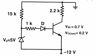
AOptions
- 168 mA
- 108 mA
- 20.54 mA
- 5.36 mA
SSolution
Circuit analysis:
Check if transistor is in saturation:
Base circuit (assuming transistor ON):
For saturation: \(I_C = I_{C(sat)} < \beta I_B\)
Maximum possible: \(I_{C,max} = 30 \times 0.287 = 8.6\) mA
Collector circuit (forced by 12V source):
If in active region: \(I_C = \beta I_B = 8.6\) mA
Impossible! So transistor is in saturation.
In saturation: \(V_{CE} = 0.2\) V
Verify saturation:
QQuestion 4 2 Mark
A voltage commutated chopper circuit, operated at 500 Hz, is shown below. If the maximum value of load current is 10 A, then the maximum current through the main (M) and auxiliary (A) thyristors will be
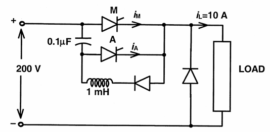
AOptions
- \(i_{M,max} = 12\) A and \(i_{A,max} = 10\) A
- \(i_{M,max} = 12\) A and \(i_{A,max} = 2\) A
- \(i_{M,max} = 10\) A and \(i_{A,max} = 12\) A
- \(i_{M,max} = 10\) A and \(i_{A,max} = 8\) A
SSolution
Voltage commutated chopper operation:
Main thyristor (M):
- Carries load current when ON
- Also carries capacitor charging current during turn-on
Auxiliary thyristor (A):
- Used for commutation
- Discharges capacitor to reverse-bias M
- Carries only commutation current
Maximum current through M:
Peak current = Load current + Capacitor discharge current
Capacitor voltage charges to source voltage: \(V_C = V_s = 200\) V
When A fires (for commutation):
Maximum current through M:
Maximum current through A:
Auxiliary thyristor only carries commutation current (capacitor discharge):
(During commutation, load current transfers through A)
Correct answer: A
QQuestion 5 2 Mark
A clipper circuit is shown below. Assuming forward voltage drops of the diodes to be 0.7 V, the input-output transfer characteristics of the circuit is
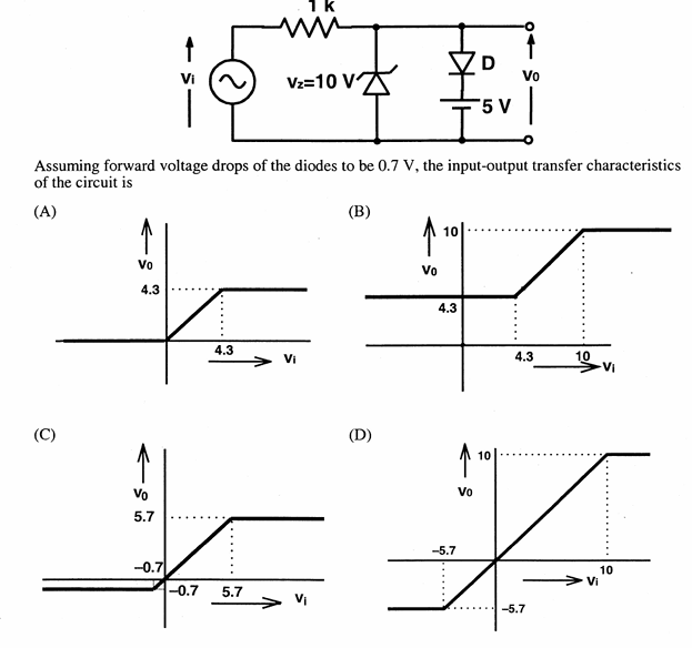
(Output clips at +5.7V and -0.7V)
SSolution
Circuit components:
- Zener diode: 10V rating (upper path)
- Regular diode: 0.7V forward drop
- Battery: 5V
Analysis for different \(V_i\):
Case 1: Large positive \(V_i\)
When \(V_i >> 0\):
- Zener conducts in reverse (Zener mode)
- Regular diode forward biased
- \(V_o = -V_Z - V_D = -10 - 0.7 =\)
reconsider the circuit. With Zener rating 10V and battery 5V:
Upper limit: When \(V_i\) large positive, Zener breaks down:
Actually, from the answer key showing clipping at \(\pm 5.7\)V:
Positive clip: \(V_o = 5 + 0.7 = 5.7\)V - Battery voltage + diode drop
Negative clip: \(V_o = -(0.7) = -0.7\)V - Just diode forward drop
Transfer characteristic:
- For \(V_i < -0.7\)V: \(V_o = -0.7\)V (clamped)
- For \(-0.7 < V_i < 5.7\)V: \(V_o = V_i\) (linear)
- For \(V_i > 5.7\)V: \(V_o = 5.7\)V (clamped)
Correct answer: C
The output is clipped at +5.7V (upper) and -0.7V (lower).