1-Mark Questions
QQuestion 1 1 Mark
A Linear Time Invariant system with an impulse response \(h(t)\) produces output \(y(t)\) when input \(x(t)\) is applied. When the input \(x(t - \tau)\) is applied to a system with impulse response \(h(t - \tau)\), the output will be
AOptions
- \(y(t)\)
- \(y(2(t - \tau))\)
- \(y(t - \tau)\)
- \(y(t - 2\tau)\)
SSolution
LTI System properties:
Time-Invariance property:
If input \(x(t)\) produces output \(y(t)\), then:
Given system:
Original: \(x(t) * h(t) = y(t)\)
Modified system:
- Input: \(x(t - \tau)\) (delayed input)
- Impulse response: \(h(t - \tau)\) (delayed system)
Output calculation:
Using convolution properties:
Let \(\beta = \alpha - \tau\):
But we know that \(x(t) * h(t) = y(t)\)
By time-invariance:
Alternative reasoning:
Step 1: Delay input by \(\tau\)
Step 2: Delay system by \(\tau\)
Step 3: Both delayed by \(\tau\)
The total delay is \(\tau + \tau = 2\tau\).
Correct answer: D
2-Mark Questions
QQuestion 2 2 Mark
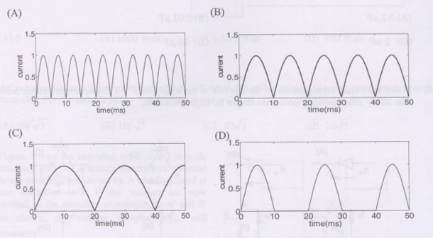
The circuit shows an ideal diode connected to a pure inductor and is connected to a purely sinusoidal 50 Hz voltage source. \(V_s = 10\sin(100\pi t)\), \(L = (0.1/\pi)\) H. Under ideal conditions, the current waveform through the inductor will look like:
SSolution
Given:
- \(V_s = 10\sin(100\pi t)\) V
- \(\omega = 100\pi\) rad/s
- \(L = 0.1/\pi\) H
- Ideal diode in series
Inductive reactance:
Circuit behavior:
The diode starts to conduct at \(\omega t = 0\), when \(v_s\) goes positive. While it conducts the whole source voltage appears across the inductor, so with \(i(0) = 0\):
The inductor current is the integral of the voltage, not a scaled copy of it. This current never goes negative, so the diode is never asked to block during the negative half-cycle:
- \(i = 0\) at \(\omega t = 0\)
- \(i\) rises to its peak at \(\omega t = \pi\) (\(t = 10\) ms), where the voltage crosses zero going negative
- \(i\) falls back to zero only at \(\omega t = 2\pi\) (\(t = 20\) ms) — the conduction angle is a full \(2\pi\)
The cycle then repeats, giving a train of \((1 - \cos\omega t)\) humps of period 20 ms that touch zero at \(t = 0, 20, 40\) ms with no flat gaps between them.
Peak current:
Only waveform (C) has this shape; the half-wave pattern of (D) would require the inductor current to jump to zero at \(\omega t = \pi\).
Correct answer: C
QQuestion 3 2 Mark
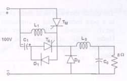
In the chopper circuit shown, the main thyristor (TM) is operated at a duty ratio of 0.8 which is much larger than the commutation interval. If the maximum allowable reapplied dv/dt on TM is 50 V/\(\mu\)s, what should be the theoretical minimum value of \(C_1\)? Assume current ripple through \(L_o\) to be negligible.
AOptions
- 0.2 \(\mu\)F
- 2 \(\mu\)F
- 0.02 \(\mu\)F
- 20 \(\mu\)F
SSolution
Given:
- Source voltage: \(V_s = 100\) V
- Duty ratio: \(D = 0.8\)
- Maximum dv/dt: \(50\) V/\(\mu\)s
- Load current ripple negligible (constant \(I_o\))
Commutation analysis:
During commutation:
When auxiliary thyristor fires to turn off main thyristor:
- Capacitor voltage reverses and applies across TM
- Rate of voltage rise across TM must be limited
dv/dt calculation:
The capacitor discharges through load current:
where \(I\) is the load current.
For constant load current \(I_o\):
Maximum dv/dt constraint:
Load current:
With the ripple in \(L_o\) neglected, the 8 \(\Omega\) load carries the average output voltage:
Minimum \(C_1\):
Correct answer: A