Electronic Devices & Circuits · Lecture 38

Thyristors: Types, Working Principles, Characteristics & Applications

Thyristors & Power Devices

Dr. Mithun Mondal BITS Pilani, Hyderabad Campus

Thyristors: Types, Working Principles, Characteristics & Applications

Overview

  • Introduction to Thyristors
  • Thyristor Family and Types
  • Construction and Operation
  • Key Characteristics
  • Applications
  • Protection Mechanisms
  • Conclusion

What is a Thyristor?

  • A semiconductor switching device with three or more PN junctions.
  • Operates as a bistable switch: ON or OFF.
  • Requires no continuous gate bias to maintain conduction.
  • Handles high voltages (>1000 V) and currents (>1000 A).
  • Derived from Greek: Thyra ("door"), symbolizing current flow control.

Thyristor Family

  • Shockley Diode (PNPN Diode)
  • Silicon Controlled Rectifier (SCR)
  • TRIAC (Triode for Alternating Current)
  • DIAC (Diode for Alternating Current)
  • Gate Turn-Off Thyristor (GTO)
  • Light-Activated SCR (LASCR)

Note: SCR and TRIAC are widely used in power control.

Basic Construction

  • Four-layer PNPN structure.
  • Terminals:
    • Shockley Diode: Anode (A), Cathode (K).
    • SCR: Anode (A), Cathode (K), Gate (G).
    • TRIAC: Terminal 1 (A\(_1\)), Terminal 2 (A\(_2\)), Gate (G).
Diagram illustrating the PNPN layer structure and terminals of a thyristor
Thyristor PNPN structure

Shockley Diode

  • Four-layer PNPN diode (Silicon Unilateral Switch).
  • Two terminals: Anode, Cathode.
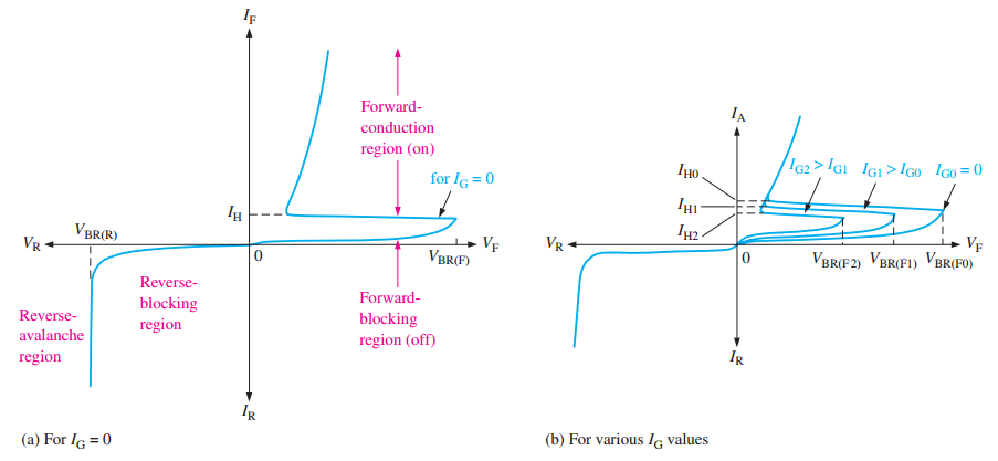
  • Turns ON when forward voltage exceeds breakover (\(V_{BR(F)}\)).
  • Exhibits latching behavior.

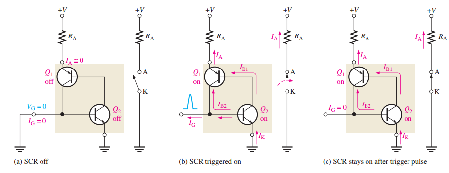
Two-Transistor Model

  • Represented as two transistors:
    • \(Q_1\): PNP transistor.
    • \(Q_2\): NPN transistor.
  • Base of \(Q_1\) connected to collector of \(Q_2\), and vice versa.
  • Provides regenerative feedback for latching.
Two-transistor equivalent model of a thyristor with regenerative feedback
Two-transistor model of a thyristor

Working Principle

  • OFF state: High resistance, minimal leakage current.
  • Triggered ON by:
    • Forward voltage exceeding breakover (\(V_{BR(F)}\)).
    • Gate pulse (for SCR, TRIAC, GTO).
  • ON state: Low resistance, latches until current drops below holding current (\(I_H\)).
Graph showing thyristor switching characteristics during turn-on process
Thyristor switching characteristics
IV curve of thyristor showing forward and reverse blocking regions
Thyristor IV characteristics

Operating Regions and Key Characteristics

Region Condition Behavior
Off (Forward Blocking) \(I_A < I_S\) High resistance, OFF
On (Forward Conduction) \(I_A > I_S\) Low resistance, ON
Turn-Off \(I_A < I_H\) Returns to OFF state

Silicon Controlled Rectifier (SCR)

Schematic symbol and circuit configuration of an SCR
SCR schematic and circuit

SCR Equivalent Circuit

Equivalent circuit of SCR using two-transistor model with gate control
SCR two-transistor equivalent circuit

Turning SCR ON (Gate Triggering)

Circuit diagram illustrating SCR gate triggering mechanism
SCR gate triggering circuit

SCR Characteristic Curves

Characteristic curves of SCR showing various operating regions
SCR characteristic curves

SCR Rectifiers

Circuit diagram of SCR full-wave rectifier with center-tapped transformer
SCR full-wave rectifier circuit

SCR Rectifier Waveforms

Waveforms of SCR rectifier showing conduction angles
SCR rectifier output waveforms

SCR Half-Wave Rectifier: Average & RMS Output Voltages

Given: \(V = V_m \sin \omega t\), conduction from \(\theta\) to \(\pi\)

\[\begin{aligned} V_{\mathrm{av}} & = \frac{1}{2\pi} \int_\theta^\pi V_m \sin \omega t \, d(\omega t) \\ &= \frac{V_m}{2\pi}(1 + \cos \theta) \end{aligned}\]
Average output voltage:

RMS output voltage:

\[\begin{aligned} V_{\mathrm{rms}} & = \sqrt{ \frac{1}{2\pi} \int_\theta^\pi (V_m \sin \omega t)^2 \, d(\omega t) } \\ & = \frac{V_m}{2} \left[ \frac{1}{\pi}(\pi - \theta + \sin 2\theta) \right]^{\frac{1}{2}} \end{aligned}\]

Special case:

SECTION 01

SCR Full-Wave Rectifier - Average Output Voltage

Given: \(V = V_m \sin \omega t\), SCRs conduct from \(\theta\) to \(\pi\) in each half

\[ V_{\mathrm{av}} = \frac{1}{\pi} \int_\theta^\pi V_m \sin \omega t \, d(\omega t) = \frac{V_m}{\pi}(1 + \cos \theta) \]
Average output voltage:

TRIAC (Triode for Alternating Current)

Schematic symbol and circuit configuration of a TRIAC
TRIAC schematic and circuit

Bilateral Operation of a TRIAC

Diagram showing bidirectional conduction paths in TRIAC operation
TRIAC bidirectional conduction

DIAC (Diode for Alternating Current)

Schematic symbol and characteristic curve of a DIAC
DIAC symbol and characteristics

Gate Turn-Off Thyristor (GTO)

Schematic symbol and structure of a GTO thyristor
GTO thyristor symbol and structure

Working Principle and Characteristics of GTO

Characteristic curves of GTO thyristor showing turn-off capability
GTO characteristic curves

Light Activated SCR (LASCR)

Structure and schematic symbol of a Light Activated SCR (LASCR)
LASCR structure and symbol

Comparison of Thyristor Family Devices

Device Control Terminal Turn-On Method Turn-Off Method Switching Speed Applications
SCR (Silicon Controlled Rectifier) Gate Gate pulse or forward breakover Natural or forced commutation Slow AC motor control, rectifiers
Triac Gate Gate pulse (positive or negative) Current goes below holding current Moderate Light dimmers, fan regulators
Diac None Breakover voltage Current goes below holding current Moderate Triggering device for Triac
GTO (Gate Turn-Off Thyristor) Gate Gate pulse Negative gate pulse Faster than SCR Choppers, inverters
IGCT (Integrated Gate-Commutated Thyristor) Gate Gate pulse Gate pulse withdrawal High High-power drives, FACTS
PUT (Programmable Unijunction Transistor) Gate Programmable voltage Current goes below holding current High Oscillators, timers
LASCR (Light Activated SCR) None or Gate Exposure to light (or gate pulse) Natural or forced commutation Moderate HVDC transmission, optical triggering

Thyristors vs. Power FETs

Feature Thyristors Power FETs
Switching Bistable (ON/OFF) Linear/ON/OFF
Current Rating Very High (>1000 A) Moderate to High
Control Signal Gate Pulse Voltage-Controlled
Bidirectional Available (TRIAC) Mostly Unidirectional
Switching Speed Slower Faster

Thyristor Protection

Circuit diagram of thyristor protection mechanisms
Thyristor protection circuit

Snubber Circuit for \(dv/dt\) Protection

Snubber circuit diagram for dv/dt protection in thyristors
Snubber circuit for dv/dt protection

Conclusion