Semiconductor diode biasing

Demonstrative Video


Semiconductor Diode

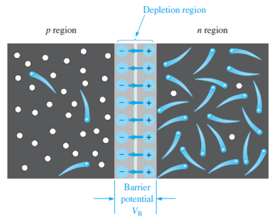
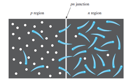
  • Intrinsic silicon doped so that one half is n-type and other half p-type forming pn junction between the two regions

  • n-region : free electrons (majority) and holes (minority) carriers

  • p-region : holes (majority) and free electrons (minority) carriers
image

  • For every \(e\) that diffuses across the junction and combines with a hole, a +ve charge is left in the n region and a -ve charge is created in the p region, forming a barrier potential, \(V_B\)

image

Biasing the Diode

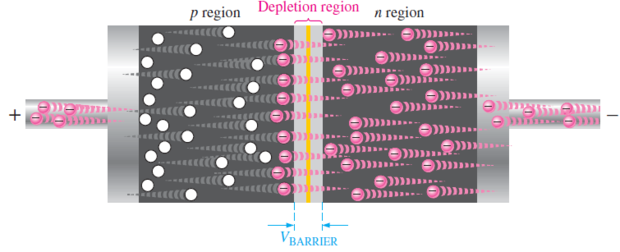
Forward Biasing

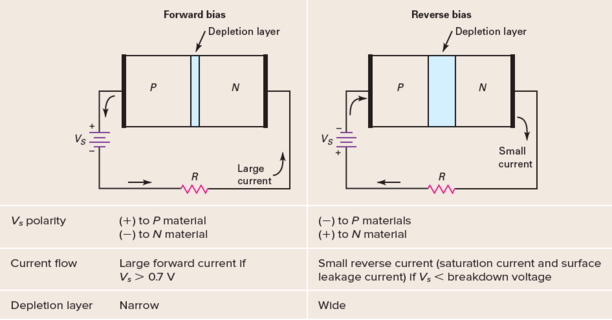
  • Source -ve terminal to n-type material, and +ve terminal to p-type material.

image

Reverse Biasing

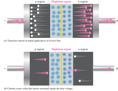
  • Battery -ve terminal connected to p side and +ve to the n side.

  • -ve terminal attracts holes, and +ve attracts free electrons causing them to flow away from the junction widening the depletion layer

image

image

PEAK INVERSE VOLTAGE (PIV)

REVERSE BREAKDOWN