Introduction
-
Operational amplifiers are fundamental building blocks in electronics
-
Basic and special purpose op-amp circuits:
-
Comparators
-
Summing amplifiers
-
Integrators and differentiators
-
Instrumentation amplifiers
-
Specialized amplifiers (OTA, log/antilog)
-
-
Applications include signal processing, digital circuits, and analog-to-digital conversion
Comparators
-
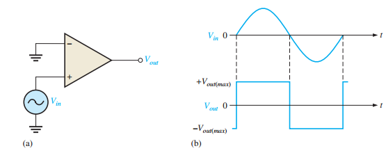
Specialized op-amp circuit that compares two input voltages
-
Output is always in one of two states (high or low)
-
Key characteristics:
-
Very fast switching times (as low as 500 ps propagation delay)
-
High open-loop gain enables detection of tiny input differences
-
-
Used for analog-to-digital interfacing
Zero-Level Detection
-
Inverting input grounded (0 V reference)
-
Input signal applied to noninverting input
-
Smallest input difference drives amplifier to saturation
-
Can convert sine waves to square waves (squaring circuit)
Nonzero-Level Detection
-
Fixed reference voltage replaces ground at inverting input
-
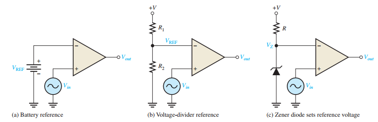
Three reference voltage methods:
-
Battery reference
-
Voltage divider reference (\(V_{REF} = \dfrac{R_2}{R_1+R_2}(+V)\))
-
Zener diode reference (\(V_{REF} = V_Z\))
-
-
Output switches when input crosses \(V_{REF}\)
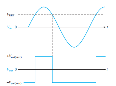
Given \( R_1 = 8.2k\Omega \), \( R_2 = 1.0k\Omega \), \( +V = 15V \):
\[ V_{REF} = \frac{1.0k\Omega}{8.2k\Omega + 1.0k\Omega}(15V) = 1.63V \]
Output switches between \( \pm 14V \) when input crosses 1.63V.
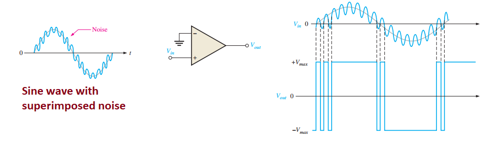
Noise Effects and Hysteresis
-
Noise (unwanted voltage fluctuations) can cause unstable switching near the threshold
-
Example: A low-frequency sinusoidal voltage with noise causes erratic output
-
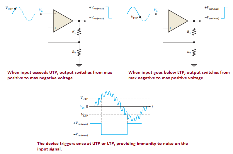
Solution: Implement hysteresis using positive feedback
-
Upper Trigger Point (UTP): \(V_{UTP} = \dfrac{R_2}{R_1+R_2}(+V_{out(max)})\)
-
Lower Trigger Point (LTP): \(V_{LTP} = \dfrac{R_2}{R_1+R_2}(-V_{out(max)})\)
-
Hysteresis voltage: \(V_{HYS} = V_{UTP} - V_{LTP}\)
-
-
Also called a Schmitt trigger
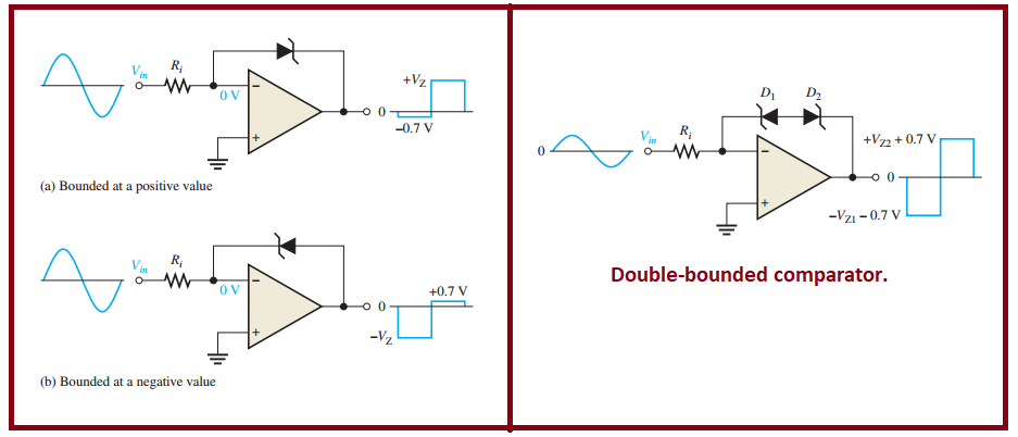
Output Bounding
-
Limits output voltage to values less than op-amp saturation
-
Methods:
-
Single zener diode: bounds one direction
-
Two zener diodes: bounds both directions (\(V_Z + 0.7V\) each way)
-
-
Example: With 4.7V zeners, output bounds at \(\pm5.4V\)
Comparator Applications
-
Over-temperature sensing:
-
Uses Wheatstone bridge with thermistor
-
Comparator detects bridge balance point
-
Triggers alarm/response when temperature exceeds threshold
-
-
Analog-to-Digital Conversion (Flash ADC):
-
Uses parallel comparators with reference voltage ladder
-
\(2^n-1\) comparators needed for n-bit conversion
-
Priority encoder produces binary output
-

Amplifiers
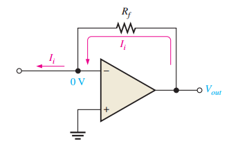
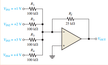
Summing Amplifier
-
Application of inverting op-amp configuration
-
Output proportional to negative sum of input voltages
-
General output equation:\[\begin{aligned} V_{OUT} = -\left(\dfrac{R_f}{R_1}V_{IN1} + \dfrac{R_f}{R_2}V_{IN2} + \cdots + \dfrac{R_f}{R_n}V_{INn}\right) \end{aligned}\]
-
For equal input resistors\[\begin{aligned} V_{OUT} = -\dfrac{R_f}{R}(V_{IN1} + V_{IN2} + \cdots + V_{INn}) \end{aligned}\]

Unity-Gain Summing Amplifier
-
Special case where \(R_f = R\)
-
Output is simple inverted sum of inputs:\[\begin{aligned} V_{OUT} = -(V_{IN1} + V_{IN2} + \cdots + V_{INn}) \end{aligned}\]
-
Example: For inputs +2V, -3V, and +4V:\[\begin{aligned} V_{OUT} = -(2V - 3V + 4V) = -3V \end{aligned}\]
Averaging Amplifier
-
Produces mathematical average of input voltages
-
Set \(R_f/R = 1/n\) where \(n\) is number of inputs
-
Output equation:\[\begin{aligned} V_{OUT} = -\dfrac{1}{n}(V_{IN1} + V_{IN2} + \cdots + V_{INn}) \end{aligned}\]
-
: , Example: 4-input averager with\[\begin{aligned} V_{OUT} = -\dfrac{25k\Omega}{100k\Omega}(V_1 + V_2 + V_3 + V_4) = -\dfrac{1}{4}(V_1 + V_2 + V_3 + V_4) \end{aligned}\]
Digital-to-Analog Conversion
-
Binary-weighted resistor DAC:
-
Each input resistor corresponds to binary weight
-
MSB has smallest resistor (\(R\)), next has \(2R\), then \(4R\), etc.
-
Output is analog representation of digital input
-
-
R/2R ladder DAC:
-
Uses only two resistor values (\(R\) and \(2R\))
-
More practical for IC implementation
-
Each bit contributes half the voltage of the previous bit
-

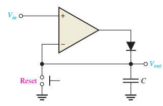
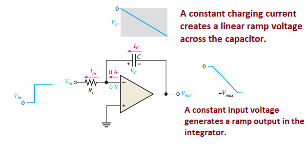
Op-Amp Integrator
-
Produces output proportional to integral of input
-
Basic configuration:
-
Input resistor \(R_{in}\)
-
Feedback capacitor \(C\)
-
-
Output voltage:\[\begin{aligned} V_{OUT} = -\dfrac{1}{R_{in}C}\int V_{IN} dt \end{aligned}\]
-
Constant input produces linear ramp output
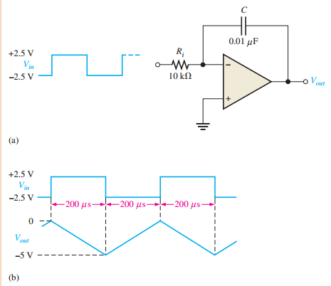
Op-Amp Integrator Example
Given \( R_{in} = 10k\Omega \), \( C = 0.01\mu F \), square wave input \( \pm 2.5V \):
\[ \frac{\Delta V_{out}}{\Delta t} = -\frac{V_{in}}{R_{in}C} = -\frac{2.5V}{10k\Omega \times 0.01\mu F} = -25mV/\mu s \]
Produces triangular wave output with 5V peak-to-peak.
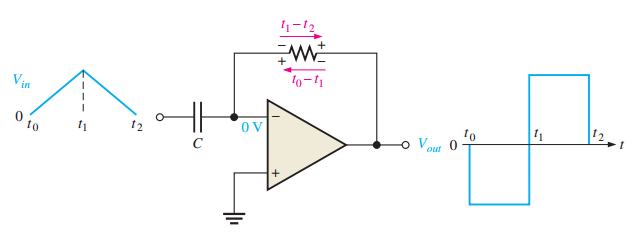
Op-Amp Differentiator
-
Produces output proportional to derivative of input
-
Basic configuration:
-
Input capacitor \(C\)
-
Feedback resistor \(R_f\)
-
-
Output voltage:
-
\[\begin{aligned} V_{OUT} = -R_f C \dfrac{dV_{IN}}{dt} \end{aligned}\]
-
Ramp input produces constant output
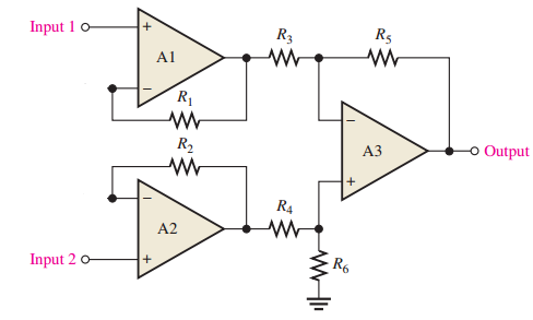
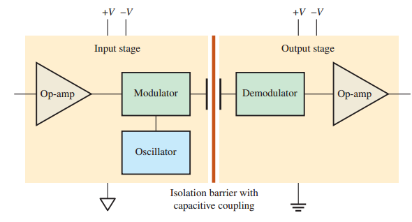
Instrumentation Amplifiers
-
Amplify small signals riding on large common-mode voltages
-
Key Characteristics:
-
High input impedance
-
High common-mode rejection
-
Low output offset
-
Low output impedance
-
-
\[\begin{aligned} \text{Gain}~A_{cl} = 1 + \dfrac{2R}{R_{\text{gain}}} \quad \text{where} \quad R_1 = R_2 = R \end{aligned}\]
-
Input Stage (2 Op-Amps): High \(Z_{in}\) and initial amplification
-
Difference Amplifier (3rd Op-Amp): Subtracts and amplifies input signal difference