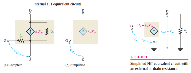
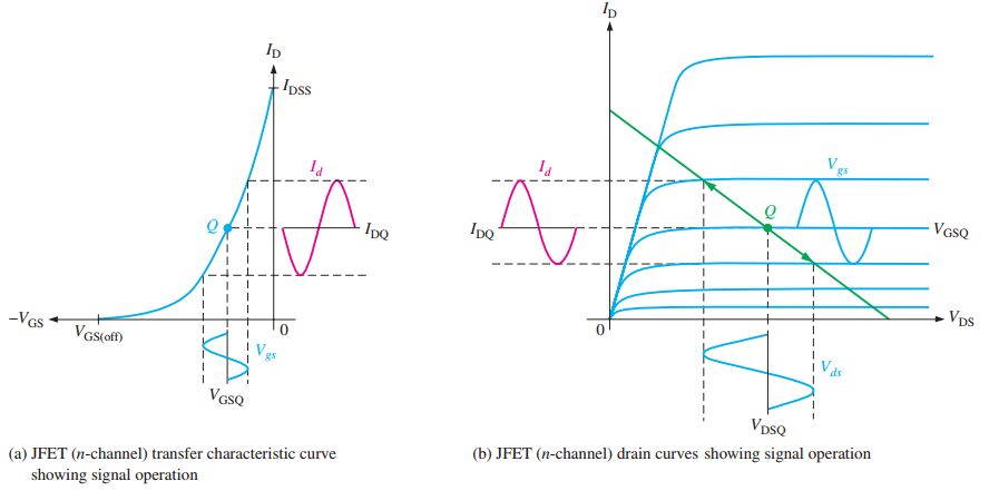
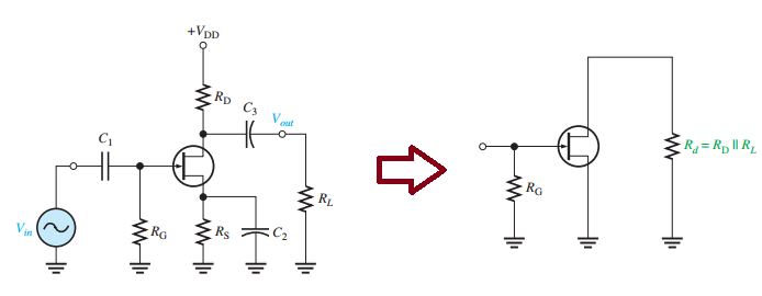
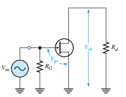
Introduction
-
FET amplifiers are preferred for:
-
High input resistance
-
Low noise
-
Low power consumption
-
-
Widely used in:
-
Communication receivers
-
Switching circuits
-
Digital and analog systems
-
FET vs BJT Amplifiers
FET
-
Voltage-controlled
-
High input impedance
-
Lower gain
-
Low noise
BJT
-
Current-controlled
-
Moderate input impedance
-
Higher gain
-
Better linearity
FET Amplifier Configurations
-
Common-Source (CS): High voltage gain, inverted output
-
Common-Drain (CD): Unity gain, no inversion (buffer)
-
Common-Gate (CG): Gain with no inversion, low input impedance
Amplifier Classes with FETs
-
Class A: Linear operation, low distortion
-
Class B and AB: Improved efficiency
-
Class C: High efficiency, used in RF
-
Class D: Switching amplifier, very efficient
Note: FETs dominate in Class D due to superior switching performance
Switching and Digital Applications
-
FETs are ideal for:
-
Analog/digital switches
-
CMOS logic circuits
-
Multiplexers, switched-capacitor circuits
-
-
Enhancement-mode MOSFETs are widely used in CMOS
FET Characteristics and Modeling
-
Voltage-controlled: Gate voltage controls drain current
-
Transconductance \(g_m = \frac{\Delta I_D}{\Delta V_{GS}}\)
-
AC Modeling: Simpler than BJT models
-
Impedance:
-
Input: Very high
-
Output: Comparable to BJT
-
Application Areas
-
Low-noise amplifiers
-
RF and high-frequency designs
-
Buffering and signal interfacing
-
Power switching and control
THE COMMON-SOURCE AMPLIFIER
FET AC Model
-
\(r_{gs}^{\prime}\) and \(r_{ds}^{\prime}\) are very high so neglected in the simplified circuit.
- The voltage gain :
Introduction to Common-Source JFET Amplifier
-
A common-source JFET amplifier is characterized by:
-
AC input at the gate.
-
AC output from the drain.
-
The source terminal is common to both.
-
-
Source is at AC ground:
-
No source resistor, or a bypassed one.
-
Ensures the amplifier gain is maximized.
-
Self-Biased JFET Configuration
-
Circuit Overview :
-
Input signal coupled via capacitor to the gate.
-
\(R_G\) ensures:
-
Gate is held near 0 V (since \(I_{GSS} \approx 0\)).
-
Very high input resistance \(\rightarrow\) avoids loading the signal source.
-
-
-
Bias voltage appears across \(R_S\), and bypass capacitor \(C_2\) ensures:
-
Source is at AC ground.
-
Signal Operation
-
Gate-source voltage swings about its Q-point \(V_{GSQ}\).
-
As \(V_{GS}\) becomes less negative, \(I_D\) increases.
-
As \(I_D\) increases, \(V_D\) drops (since \(V_D = V_{DD} - I_D R_D\)).
-
Result:
-
\(V_{DS}\) is 180° out of phase with \(V_{GS}\).
-
This is characteristic of a common-source amplifier.
-
Graphical Illustration
-
Transfer Characteristic Curve :
-
Sinusoidal \(V_{GS}\) causes sinusoidal \(I_D\).
-
-
Drain Curve : Signal causes Q-point to shift along the load line.
-
Nonlinear nature of transfer curve causes distortion.
-
Minimize distortion: Keep signal swing within a limited range on the load line.
DC Analysis – Graphical and Mathematical Approaches
-
Objective: Find Q-point \((I_D, V_{GS})\)
-
Graphical Method:
-
Use transconductance curve.
-
Plot load line: Intersection gives Q-point.
-
-
Mathematical Method:
- Based on the relation:
-
This results in a quadratic equation in \(I_D\).
AC Analysis – Equivalent Circuit
-
Replace capacitors with shorts (AC coupling).
-
Replace \(V_{DD}\) with AC ground.
-
Resulting AC equivalent circuit:
-
Drain and source both tied to AC ground.
-
Gate Signal and Input Resistance
-
: appears at the Almost all of
-
Very high input resistance:
-
Due to reverse-biased gate–source junction.
-
- Total input resistance:
Voltage Gain of Common-Source Amplifier
- Voltage Gain:
- Output Voltage:
- Where:
-
Important Note:
-
\(V_{\text{out}}\) is 180° out of phase with \(V_{\text{in}}\)
-
Hence, \(A_v\) is negative.
-
Summary of Common-Source JFET Amplifier
-
Advantages:
-
High input resistance.
-
Voltage amplification with phase inversion.
-
- Key Equations
-
Design Consideration:
-
Ensure Q-point lies in the linear region for undistorted amplification.
-
D-MOSFET Amplifier Operation
-
Configuration: Zero-biased common-source n-channel D-MOSFET
-
DC Conditions:
-
Gate at \(0 \, \text{V dc}\)
-
Source grounded \(\rightarrow\) \(V_{GS} = 0 \, \text{V} \Rightarrow I_D = I_{DSS}\)
-
-
Signal Behavior:
-
\(V_{gs}\) swings above and below 0 V
-
Negative swing \(\rightarrow\) Depletion mode \(\rightarrow\) \(I_D \downarrow\)
-
Positive swing \(\rightarrow\) Enhancement mode \(\rightarrow\) \(I_D \uparrow\)
-
- DC Output Voltage
-
AC Analysis: Same as in JFET amplifier
E-MOSFET Amplifier Operation
-
Configuration: Common-source n-channel E-MOSFET with voltage-divider bias
- to ensure: Gate is
-
Signal Swing :
-
\(V_{gs}\) varies around \(V_{GSQ}\)
-
\(I_D\) swings around \(I_{DQ}\)
-
Operation stays in enhancement mode
-
DC Analysis for E-MOSFET
- Gate Voltage
- Drain Current
- Drain-to-Source Voltage
AC Analysis and Input Resistance
- Voltage Gain
- AC Input Resistance
- Where:
Comparison of JFET, D-MOSFET, and E-MOSFET
Characteristic | JFET | D-MOSFET | E-MOSFET |
---|---|---|---|
Full Form | Junction Field Effect Transistor | Depletion-mode Metal-Oxide-Semiconductor FET | Enhancement-mode Metal-Oxide-Semiconductor FET |
Channel Type | Physically present (n or p) | Physically present (n or p) | Not present initially; formed by VGS |
Operation Mode | Only depletion mode | Depletion and enhancement modes | Only enhancement mode |
Gate-Source Voltage (VGS) | Negative (n-channel), Positive (p-channel) | 0, negative, or positive | Must be positive (n-channel) or negative (p-channel) |
Gate Current | Small (reverse-biased pn junction) | Very small (insulated gate) | Very small (insulated gate) |
Input Impedance | High (less than MOSFETs) | Very high | Very high |
Control Mechanism | Gate voltage controls channel width | Modulates conductivity of existing channel | Gate voltage induces channel |
Turn-on Behavior | Conducts at VGS = 0 V | Conducts at VGS = 0 V | Requires threshold VGS to turn ON |
Symbol Difference | Gate arrow touches channel | Arrow does not touch (bar in symbol) | Arrow does not touch channel |
Manufacturing Complexity | Simpler | More complex | Most complex |
Applications | Low-noise amplifiers, analog circuits | Analog and RF circuits | Digital circuits, power switching |
The Common-Drain (CD) Amplifier
-
Also known as a Source-Follower (analogous to the Emitter-Follower in BJT)
-
Circuit Example:
-
Self-biased JFET
-
\(\mathbf{C_1}/\mathbf{C_2}\): Input/Output coupling capacitor
-
-
Key Characteristics:
-
Input: Gate and Output: Source
-
Drain is common to both input and output \(\rightarrow\) No drain resistor needed
-
Output voltage follows input: \(V_{\text{source}} \approx V_{\text{gate}}\) (in phase)
-
Voltage Gain of Source-Follower
-
Observation:
-
\(A_v < 1\), always slightly less
-
If \(g_m R_S \gg 1\), then \(A_v \approx 1\)
-
No phase inversion: Output is in-phase with input
-
Input Resistance of CD Amplifier
-
As in common-source configuration:
-
Gate is reverse-biased \(\rightarrow\) Very high input resistance
-
- Total input resistance:
- Where:
-
Conclusion:
-
\(R_{\text{in}}\) is typically very large, dominated by \(R_G\)
-
Excellent for buffering applications due to high input, low output impedance
-
The Common-Gate (CG) Amplifier
-
Analogous to: Common-Base (CB) BJT amplifier
-
Key Features:
-
Input: Source terminal
-
Output: Drain terminal
-
Gate is common \(\rightarrow\) connected to ground
-
Low input resistance (unlike CS and CD configurations)
-
-
Circuit Reference:
-
Self-biased configuration
-
\(\mathbf{C_1}/\mathbf{C_2}\): Input/Output coupling capacitor
-
Voltage Gain of CG Amplifier
- Starting from definition:
- Final expression:
-
Where: \(R_d = R_D \parallel R_L\)
-
Observation:
-
Same gain expression as common-source amplifier
-
No phase inversion (output in phase with input)
-
Input Resistance of CG Amplifier
-
Unlike CS and CD (which use gate as input), CG uses source as input:
- Input current
- Input voltage
- Therefore:
-
Conclusion:
-
Low input resistance
-
Suitable for low-impedance signal sources
-
Introduction to Class D Amplifier
-
Uses: Primarily MOSFETs, not BJTs or linear-mode FETs
-
Fundamental difference:
-
Operates with switching transistors (ON/OFF)
-
Not linear amplification like Class A, B, or AB
-
-
Key advantage:
-
Theoretical Efficiency:\(100\%\)
-
Practical Efficiency: \(> 90\%\)
-
Compared to:
-
Class A: \(\sim 25\%\)
-
Class B/AB: \(\sim 79\%\)
-
-
-
Block Diagram:
-
Pulse-width modulator → MOSFET switch stage → Low-pass filter → Speaker
-
Pulse-Width Modulation (PWM)
-
PWM: Converts analog input to pulses of varying width
-
Wider pulse = Higher input amplitude
-
Narrower pulse = Lower input amplitude
-
Zero input = Square wave output
-
Generated using: Comparator
-
Comparator Behavior:
-
Outputs high or low depending on input polarity
-
Operates with a sine wave (input) and triangular wave (carrier)
-
Output swings rail-to-rail (e.g., \(\pm 12\) V to \(\pm 24\) V)
-
Frequency Spectrum of PWM
-
PWM spectrum includes:
-
Input signal frequency (\(f_{in}\))
-
Modulator frequency (\(f_m\))
-
Harmonics above and below \(f_m\)
-
-
Requirement:
-
\(f_m\) must be much higher than max \(f_{in}\)
-
-
Why?
-
To easily filter out harmonics
-
Pass only the original input signal through the low-pass filter
-
Power Stage & Switching
-
MOSFET Configuration:
-
Complementary push-pull
-
Operate in ON/OFF mode, not linear
-
-
Switching logic:
-
When \(Q_1\) is ON \(\rightarrow\) \(Q_2\) is OFF and vice versa
-
ON: High current, low voltage drop \(\rightarrow\) Low power dissipation
-
OFF: No current \(\rightarrow\) No power dissipation
-
-
Power dissipation occurs only during switching transitions
Efficiency of Class D
-
Ideal Power Dissipation:
-
\(P_{DQ1} = 0 \, \text{W}\), \(P_{DQ2} = 0 \, \text{W}\)
-
- Output Power
- Maximum Efficiency
-
Practical Limitations:
-
Small \(V_{DS(on)}\)
-
Switching losses
-
Losses in comparators & wave generator
-
Signal Flow in Class D Amplifier
-
Stages:
-
Small analog audio input
-
PWM modulator (Comparator + triangle wave)
-
MOSFET switching stage (with gain)
-
Low-pass filter \(\rightarrow\) Removes PWM carrier & harmonics
-
Amplified analog output to speaker
-