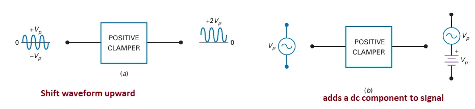
Positive Clamper Circuit
Clamper vs. Clamp:
Clamper: Adds a DC voltage to the signal
Clamp: Protects sensitive circuits by limiting voltage
Positive Clamper:
Operation:
Shifts the AC reference level up to a DC level
AC signal centered on a positive DC level
Effect:
Each point on the sine wave is shifted upward
Positive peak: \(2V_p\), Negative peak: \(0\) V
Working Principle:
Capacitor Charging:
Initially uncharged capacitor
On the first negative half-cycle, the diode conducts
Capacitor charges to \(V_p\)
Stiff Clamper:
\(R_L C > 100T\) ensures the capacitor remains charged
Acts like a battery of \(V_p\) volts
Produces a positively clamped signal
Real-World Consideration:
Diode drop of 0.7 V during conduction
Output reference level slightly below zero at \(-0.7\) V

Negative Clamper Circuit
Negative Clamper:
Operation:
Diode reversed from the positive clamper configuration
Capacitor voltage reverses, resulting in a negative clamping effect
Sine wave shifts downward, creating a negative clamping
Clamping Level:
Positive peaks have a reference level of \(+0.7\) V instead of 0 V
Diode Orientation as Memory Aid:
Diode points in the direction of the waveform shift
Negative Clamper: Diode points down, waveform shifts down
Positive Clamper: Diode points up, waveform shifts up

Applications:
Widely used in television receivers to adjust video signal reference levels
Also found in radar and communication circuits
Imperfections:
Less-than-perfect clamping due to the diode’s barrier potential
Solutions involving op amps will be discussed later to achieve near-perfect clamping