Basic Concepts
Amplifiers behave differently at low, mid, and high frequencies.
Coupling and bypass capacitors appear as shorts at midband frequencies.
At low frequencies, capacitive reactance affects gain and phase shift.
Frequency response: Change in gain or phase shift over a range of input frequencies.
Effects of Circuit Capacitances
Coupling capacitors:
\(X_C = \dfrac{1}{2\pi fC}\)
Higher reactance at low frequencies reduces gain.
Introduces phase shift (lead circuit).
Bypass capacitors:
At low frequencies, \(X_C\) becomes significant.
Emitter/source is no longer at AC ground.
Reduces gain due to impedance formed with \(R_E\) or \(R_S\).
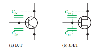
Internal Transistor Capacitances
At high frequencies, coupling/bypass capacitors are shorts.
Internal capacitances (\(C_{be}, C_{bc}\) for BJT; \(C_{gs}, C_{gd}\) for FET) dominate.
Reduce gain and introduce phase shift as frequency increases.
Datasheet notations:
BJT: \(C_{ib}\) (input), \(C_{ob}\) (output).
FET: \(C_{iss}\) (input), \(C_{rss}\) (reverse transfer).
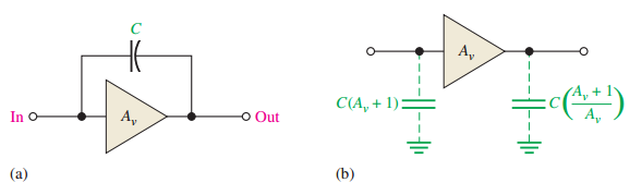
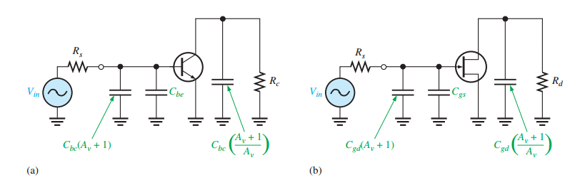
Miller’s Theorem
Used to simplify high-frequency analysis of inverting amplifiers.
- Miller input capacitance:\[C_{in(Miller)} = C_{bc}(A_v + 1)\]
- Miller output capacitance:\[C_{out(Miller)} = C_{bc}\left(\dfrac{A_v + 1}{A_v}\right)\]
For FETs, replace \(C_{bc}\) with \(C_{gd}\).
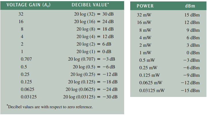
The Decibel (dB)
Logarithmic unit for gain measurement.
- Power gain in dB:\[A_p(\text{dB}) = 10 \log A_p\]
- Voltage gain in dB:\[A_v(\text{dB}) = 20 \log A_v\]
Positive dB: Gain \(> 1\)
Negative dB: Gain \(< 1\) (attenuation).
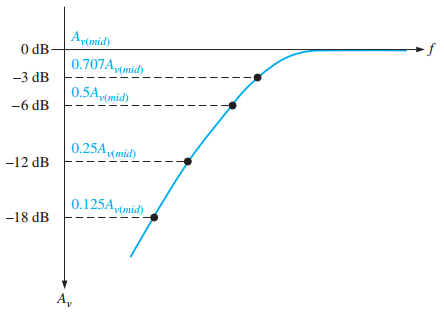
0 dB Reference and Critical Frequency
0 dB Reference: Midrange gain is assigned 0 dB; other gains are relative.
The maximum gain occurs between the lower and upper critical frequencies, known as the midrange region.
Critical frequency (cutoff frequency):
Frequency where output power drops to half (-3 dB).
Voltage gain is 70.7% of midrange value.
Power measurement in dBm
Power measurement in dBm:
Reference: 1 mW.
\(P(\text{dBm}) = 10 \log\left(\dfrac{P}{1\,\text{mW}}\right)\).
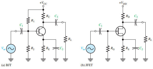
Low-Frequency Response (BJT Amplifiers)
Three high-pass RC circuits affect low-frequency gain:
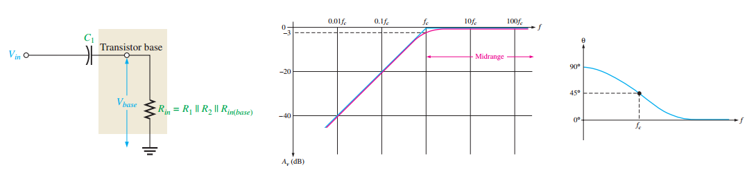
Input RC circuit (\(C_1\) and input resistance).
Output RC circuit (\(C_3\) and output resistance).
Bypass RC circuit (\(C_2\) and emitter resistance).
Each circuit has a lower critical frequency (\(f_{cl}\)).
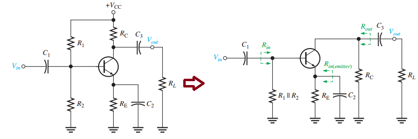
Input RC Circuit (BJT)
- Lower critical frequency:\[f_{cl(input)} = \dfrac{1}{2\pi R_{in} C_1}\]
Roll-off: -20 dB/decade below \(f_{cl}\).
- \(f \rightarrow 0\)\(90^{\circ}\)\(f_{cl}\)\(45^{\circ}\)\(0^{\circ}\)Phase shift:\[\theta = \tan^{-1}\left(\dfrac{X_{C1}}{R_{in}}\right)\]
Output and Bypass RC Circuits (BJT)
Output RC circuit:
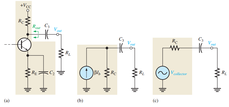
Development of the equivalent low-frequency output RC circuit.
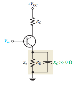
Bypass RC circuit:
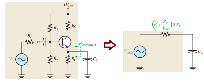
Development of the equivalent bypass RC circuit. Swamping resistor (\(R_{E1}\)) reduces effect of \(C_2\).
Low-Frequency Response (FET Amplifiers)
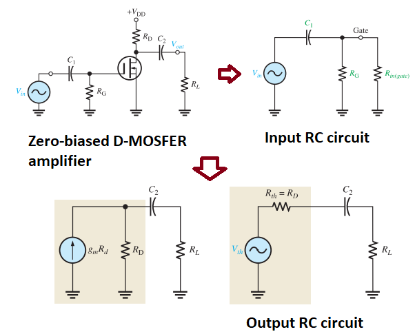
Two high-pass RC circuits:
Input RC circuit (\(C_1\) and \(R_{in} = R_G \parallel R_{in(gate)}\)).
Output RC circuit (\(C_2\) and \(R_D \parallel R_L\)).
Lower critical frequencies:
Input: \(f_{cl(input)} = \dfrac{1}{2\pi R_{in} C_1}\) Output: \(f_{cl(output)} = \dfrac{1}{2\pi (R_D + R_L) C_2}\).
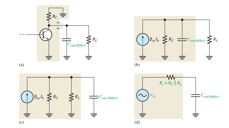
High-Frequency Response (BJT Amplifiers)
Internal capacitances (\(C_{be}, C_{bc}\)) dominate.
Miller’s theorem splits \(C_{bc}\) into input/output capacitances.
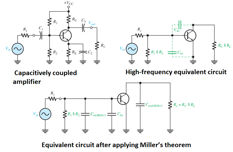
Two low-pass RC circuits:
Input RC circuit: \(C_{in(tot)} = C_{be} + C_{in(Miller)}\).
Output RC circuit: \(C_{out(Miller)} \approx C_{bc}\).
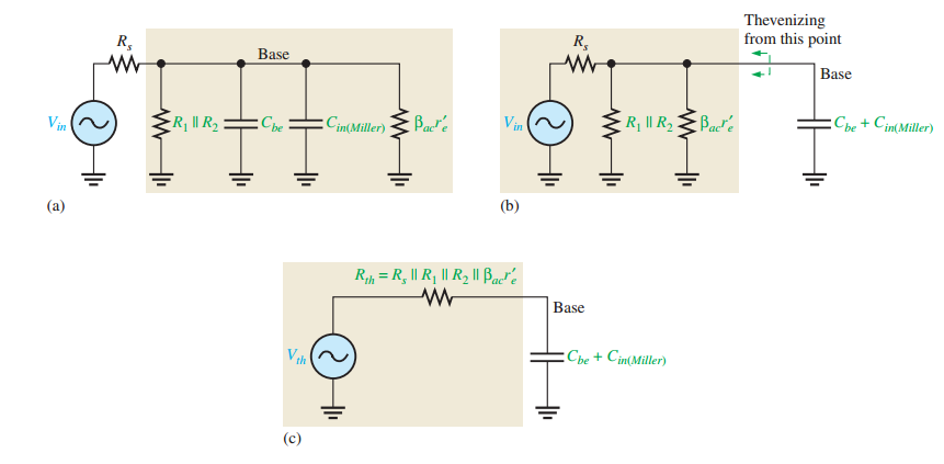
Upper Critical Frequencies (BJT)
- Input RC circuit\[f_{cu(input)} = \dfrac{1}{2\pi R_{in(tot)} C_{in(tot)}}\]
- Output RC circuit\[f_{cu(output)} = \dfrac{1}{2\pi R_c C_{out(Miller)}}\]
Phase shifts: Output lags input (up to \(90^{\circ}\)).
High-Frequency Response (FET Amplifiers)
Internal capacitances (\(C_{gs}, C_{gd}, C_{ds}\)) dominate.
Datasheet parameters:
\(C_{gd} = C_{rss}\).
\(C_{gs} = C_{iss} - C_{rss}\).
\(C_{ds} = C_{oss} - C_{rss}\).
Miller’s theorem applied to \(C_{gd}\).
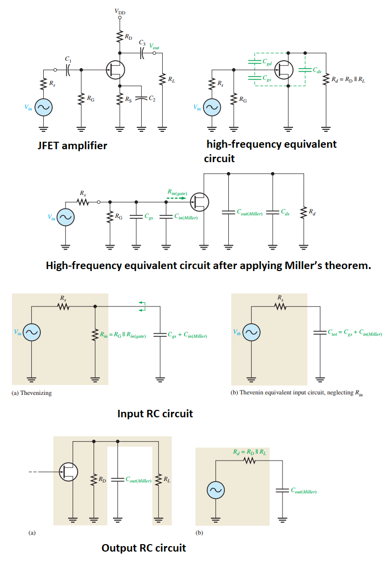
Upper Critical Frequencies (FET)
- . where Input RC circuit\[f_{cu(input)} = \dfrac{1}{2\pi R_s C_{in(tot)}}\]
- . where Output RC circuit\[f_{cu(output)} = \dfrac{1}{2\pi R_d C_{out(Miller)}}\]

Total Frequency Response
Combines low-frequency and high-frequency responses.
Dominant critical frequencies:
\(f_{cl(dom)}\): Highest lower critical frequency.
\(f_{cu(dom)}\): Lowest upper critical frequency.
- Bandwidth:\[BW = f_{cu(dom)} - f_{cl(dom)}\]
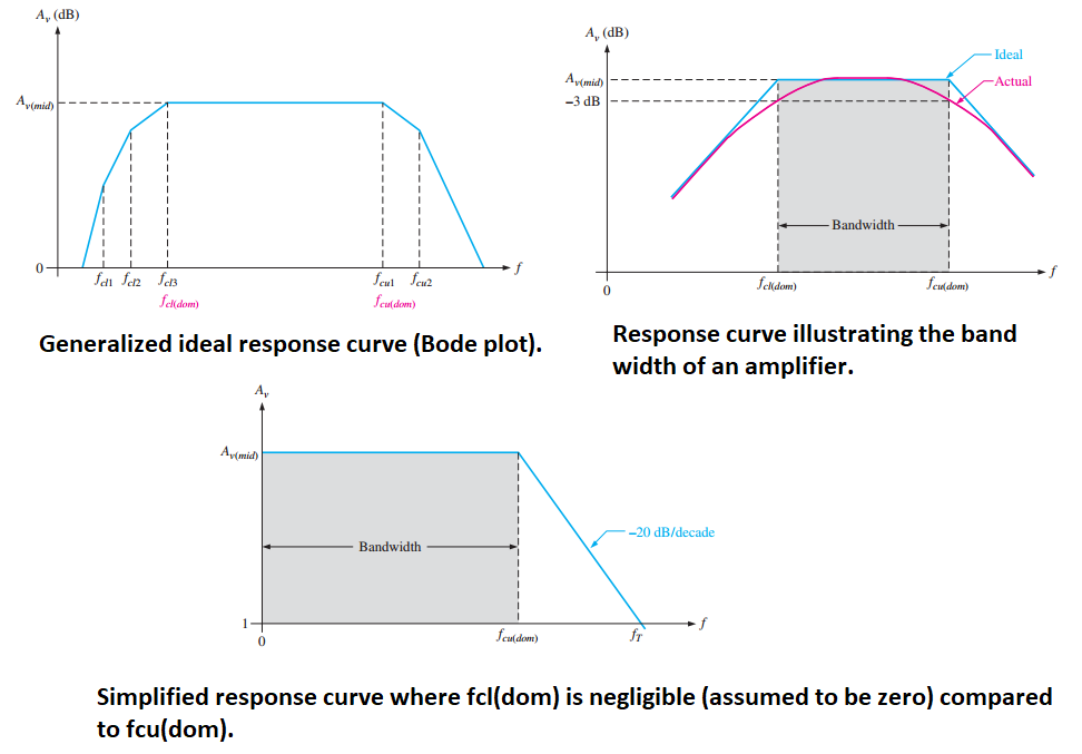
Gain-Bandwidth Product
For a given transistor, \(f_T = A_{v(mid)} \times BW\).
\(f_T\): Unity-gain frequency (gain = 1).
Constant for a given transistor.
- : , Example:\[BW = \dfrac{175\, \text{MHz}}{50} = 3.5\, \text{MHz}\]
Multistage Amplifiers
Different critical frequencies:
Overall \(f_{cl(dom)}\): Dominant \(f_{cl}\) of any stage.
Overall \(f_{cu(dom)}\): Dominant \(f_{cu}\) of any stage.
- = number of stages. where Identical stages\[f'_{cl(dom)} = \dfrac{f_{cl(dom)}}{\sqrt{2^{1/n} - 1}}\]
Measurement Techniques
Equipment:
Function generator (input signal).
Oscilloscope (measure input/output).
Procedure:
Set midrange frequency, adjust input for 1 V output.
Decrease frequency until output is 0.707 V (\(f_{cl}\)).
Increase frequency until output is 0.707 V (\(f_{cu}\)).

Summary
Amplifier response varies with frequency due to capacitive effects.
Low frequencies: Coupling/bypass capacitors reduce gain.
High frequencies: Internal transistor capacitances reduce gain.
Bandwidth is determined by dominant critical frequencies.
Multistage amplifiers have narrower bandwidth than single stages.