Overview
Demonstrative Video
Basic Electronics Contents:
-
Semiconductors
-
PN Junction Diode
-
Bipolar Junction Transistors (BJT)
Semiconductor Fundamentals
Semiconductor Materials
-
Semiconductor: are special class of elements having a conductivity between that of a good conductor and that of an insulator
-
Semiconductor materials fall into one of two classes:
-
Single crystal - germanium (Ge) and silicon (Si) having repetitive crystal structure
-
Compound - gallium arsenide (GaAs), cadmium sulphide (CdS), gallium nitride (GaN), and gallium arsenide phosphide (GaAsP) are constructed of two or more semiconductor materials of different atomic structure.
-
-
The three semiconductors used most frequently in the construction of electronic device are Ge, Si, and GaAs.
-
Best conductors (silver, copper, and gold) have one valence electron , whereas the best insulators have eight valence electrons
-
Best semiconductors have four valence electrons .
-
Many years ago, Ge was only material suitable for making semiconductor devices.
-
But Ge devices had a fatal flaw (their excessive reverse current, discussed later) that engineers could not overcome.
-
Next to oxygen, silicon is the most abundant element on the earth.
-
The advantages of Si immediately made it the semiconductor of choice.
-
Without it, modern electronics, communications, and computers would be impossible.
-
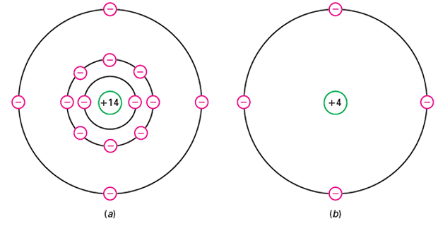
An isolated silicon atom has 14 protons and 14 electrons
-
core net charge 14 because it contains 14 protons in the nucleus and 10 electrons in the first two orbits.
Energy Band
-
The range of energies possessed by electrons of the same orbit in a solid is known as energy band .
-
In a single isolated atom, electrons revolving in any orbit possess a definite energy.
-
However in a solid, an atom is greatly influenced by the closely packed neighbouring atoms.
-
Because of this the electrons in the same orbit have a range of energies rather than a single energy.
-
Although there are number of energy bands in solids, but we are more concerned with the following:
-
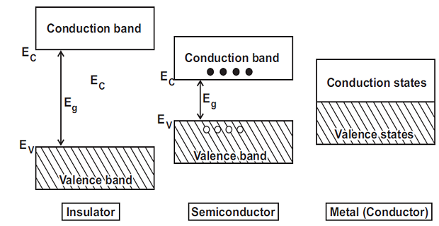
Valence band: Outermost orbit electrons in an atom, highest energy level.
-
Conduction band: Loose electrons responsible for current conduction.
-
Forbidden Energy Gap: Gap between valence and conduction bands.
-
Silicon Crystal Structure:
-
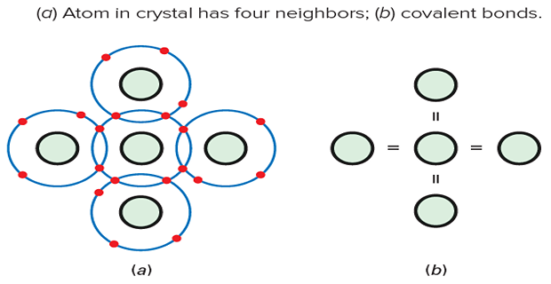
Silicon atoms arrange themselves in an orderly pattern called a crystal.
-
Each silicon atom shares its electrons with four neighbouring atoms.
-
This sharing allows each atom to have a total of eight electrons in its valence orbit.
-
Covalent bonds form between atoms due to the equal and opposite forces of attraction.
-
Billions of covalent bonds hold the silicon crystal together, giving it solidity.
-
-
Eight Electrons and Chemical Stability:
-
Each atom in a silicon crystal has eight electrons in its valence orbit.
-
This configuration results in chemical stability and solid material.
-
Elements tend to combine and share electrons to achieve eight electrons in their outer orbit.
-
The reason why eight electrons provide stability is not fully understood, but it is observed in various materials.
-
-
Scientific Laws and Explanations:
-
There are advanced physics equations that partially explain the stability of eight electrons in different materials.
-
The significance of the number eight remains unexplained, similar to other observed laws in physics, such as the law of gravity and Coulomb’s law.
-
When the valence orbit has eight electrons, it is saturated because no more electrons can fit into this orbit
-
-
Ambient Temperature and Vibrating Atoms:
-
Ambient temperature is the temperature of the surrounding air.
-
At temperatures above absolute zero ( \(-273^{\circ}\) ), the heat energy causes the atoms in a silicon crystal to vibrate.
-
Higher ambient temperatures result in stronger mechanical vibrations.
-
The warmth felt when picking up a warm object is due to the vibrating atoms.
-
-
Generation of Free Electrons and Holes:
-
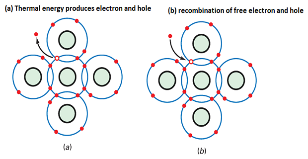
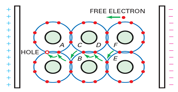
Vibrations in a silicon crystal can dislodge electrons from the valence orbit.
-
The released electron gains enough energy to move into a larger orbit, becoming a free electron.
-
The departure of the electron creates a vacancy in the valence orbit called a hole.
-
Holes behave like positive charges and can attract and capture nearby electrons.
-
The presence of holes is a critical difference between conductors and semiconductors.
-
-
Role of Doping:
-
At room temperature, thermal energy produces only a few holes and free electrons.
-
To increase the number of holes and free electrons, the crystal needs to be doped.
-
-
Recombination and Lifetime:
-
In a pure silicon crystal, thermal energy generates an equal number of free electrons and holes.
-
Free electrons move randomly throughout the crystal.
-
Occasionally, a free electron and a hole come close to each other, resulting in recombination.
-
Recombination is the merging of a free electron and a hole.
-
The time between the creation and disappearance of a free electron is called the lifetime.
-
The lifetime can vary from a few nanoseconds to several microseconds, depending on the crystal’s quality and other factors.
-
-
Main Points inside a Silicon Crystal:
-
Creation of Free Electrons and Holes:
-
Thermal energy generates some free electrons and holes.
-
-
Recombination of Free Electrons and Holes:
-
Other free electrons and holes recombine.
-
-
Temporary Existence of Free Electrons and Holes:
-
Some free electrons and holes exist temporarily, waiting for recombination.
-
-
Intrinsic Semiconductor
-
An extremely pure semiconductor is called an intrinsic semiconductor.
-
At absolute zero temperature, the valence band of an intrinsic semiconductor is completely filled, and the conduction band is completely empty.
-
When heat energy is supplied (e.g., at room temperature), some valence electrons are lifted to the conduction band, creating free-moving electrons and holes.
-
Intrinsic semiconductors have a negative temperature coefficient of resistance, meaning their resistivity decreases and conductivity increases with a rise in temperature.
Extrinsic Semiconductor
-
Extrinsic Semiconductor:
-
An intrinsic semiconductor, on its own, is not useful for electronic devices.
-
To make it conductive, a small amount of suitable impurity is added, resulting in an extrinsic (impure) semiconductor.
-
The process of adding impurities to a semiconductor is called doping, which needs to be closely controlled.
-
Extrinsic semiconductors are classified based on the type of impurity added:
-
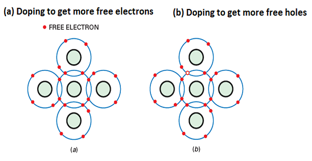
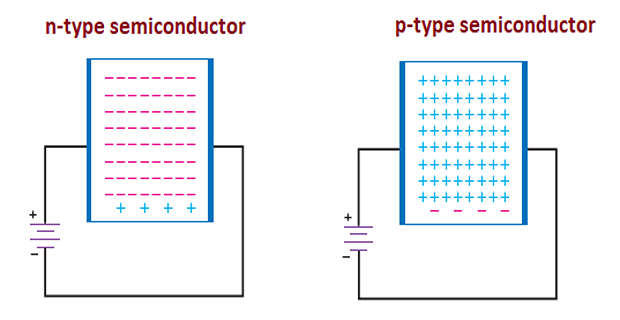
n-type semiconductor: When a donor impurity is added, creating excess free electrons.
-
p-type semiconductor: When an acceptor impurity is added, creating excess holes.
-
-
Hole flow through a semiconductor
n-type semiconductors
-
When a small amount of pentavalent impurity is added to a pure semiconductor, it creates an extrinsic semiconductor known as an n-type semiconductor.
-
Pentavalent impurities such as arsenic and antimony provide a large number of free electrons in the semiconductor crystal.
-
These impurities are called donor impurities because each atom donates one free electron to the semiconductor crystal.
-
The pentavalent impurity atoms fit into the crystal structure, with their four valence electrons forming covalent bonds and the fifth electron being free.
-
The small amount of pentavalent impurity results in a large number of free electrons available for conduction.
p-type semiconductors
-
When a small amount of trivalent impurity is added to a pure semiconductor, it creates an extrinsic semiconductor known as a p-type semiconductor.
-
Trivalent impurities such as boron, gallium and indium provide a large number of free holes in the semiconductor crystal.
-
These impurities are called acceptor impurities because each atom creates a hole that can accept an electron from the semiconductor crystal.
-
The trivalent impurity atoms fit into the crystal structure, with their three valence electrons forming covalent bonds but leaving one covalent bond incomplete, creating a hole.
-
The small amount of trivalent impurity results in a large number of holes available in the semiconductor.
Summary
-
In an n-type semiconductor , a small amount of pentavalent impurity is added, providing a large number of free electrons. These impurities are donor impurities.
-
In a p-type semiconductor , a small amount of trivalent impurity is added, providing a large number of free holes. These impurities are acceptor impurities.
Mass Action Law
-
Under thermal equilibrium, the product of the number of holes and electrons is constant and independent of the amount of donor and acceptor impurity doping.
\[\boxed{n \cdot p = n_i^2}\] -
While considering the conductivity of the doped semiconductors, only the dominant majority charge carriers have to be considered
Charge densities in doped semiconductors
-
N-type semiconductor:
\[\begin{aligned} N_D & = \text{conc. of donor atoms} \\ n_N & = \text{electron conc. in N-type} \\ p_N & = \text{hole conc. in N-type} \end{aligned}\]
-
P-type semiconductor:
\[\begin{aligned} p_P & = N_A + n_P \approx N_A \\ n_p & = \dfrac{n_i^2}{p_P}~(\text{from mass action law})\\ & \approx \dfrac{n_i^2}{N_A} \end{aligned}\]\[\begin{aligned} N_A & = \text{conc. of acceptor atoms} \\ p_p & = \text{hole conc. in P-type} \\ n_P & = \text{electron conc. in P-type} \end{aligned}\]
Extrinsic Conductivity
-
Conductivity of N-type semiconductor:\[\sigma_N = qn_N\mu_n \approx qN_D\mu_n \quad \text{since}~n_N \approx N_D\]
-
Conductivity of P-type semiconductor:\[\sigma_P= qn_P\mu_p \approx qN_A\mu_p \quad \text{since}~p_P \approx N_A\]
-
If conc. of donor atoms added to a P-type semiconductor exceeds the conc. of acceptor atoms i.e. \(N_D >> N_A\) then P-type is converted to N-type
-
Similarly, if \(N_A >> N_D\) , N-type converted to P-type
Problem
-
Find the conductivity of silicon
-
in intrinsic condition at a room temp. of \(300^{\circ}\) K
-
with donor impurity of 1 in \(10^8\)
-
with acceptor impurity of 1 in \(5\times 10^{7}\)
-
with both impurities present simultaneously
Given that
-
Solution
-
In intrinsic condition,\[\begin{aligned} \sigma_i &=q n_i\left(\mu_n+\mu_p\right) =\left(1.6 \times 10^{-19}\right)\left(1.5 \times 10^{10}\right)(1300+500) \\ &=4.32 \times 10^{-6} \mathrm{~S} / \mathrm{cm} \end{aligned}\]
-
\[\begin{aligned} p &=\frac{n_i^2}{n} \approx \frac{n_i^2}{N_D} =\frac{\left(1.5 \times 10^{10}\right)^2}{5 \times 10^{14}}=0.46 \times 10^6 \mathrm{~cm}^{-3} \end{aligned}\]\(p\) \(p \ll n\) Therefore, Further, Hence, Number of silicon atoms\[\begin{aligned} \sigma &=n q \mu_n=N_D q \mu_n \\ &=\left(5 \times 10^{14}\right)\left(1.6 \times 10^{-19}\right)(1300) \\ &=0.104 \mathrm{~S} / \mathrm{cm} . \end{aligned}\]
Drift and Diffusion Currents
-
Flow of charge (current) through a semiconductor or PN junction diode has two components:
-
Drift current
-
Diffusion current
-
-
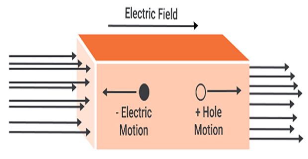
Drift current :
-
Drift current arises from the movement of carriers in response to an applied electric field.
-
Positive carriers (holes) move in the same direction as the electric field
-
Negative carriers (electrons) move in the opposite direction.
-
The net motion of charged particles generates a drift current that is in the same direction as the applied electric field.
-
-
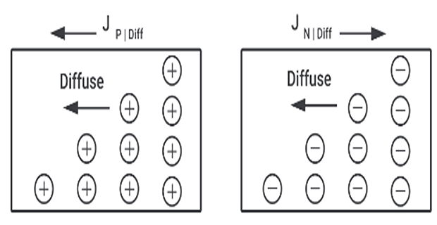
Diffusion current :
-
Electric current can flow even in the absence of applied voltage provided a concentration gradient exists
-
When the number of either electrons or holes is greater in one region than that of other region
-
Charge carrier move from higher to lower concentration of same type of charge carrier
-
Movement of charge carrier resulting in a current called diffusion current
-
-
hole density \(p(x)\) decreases with increasing \(x\) , hence negative sign
-
\(J_p\) is positive in \(+x\) direction
-
\(dn/dx\) and \(dp/dx\) are concentration gradients
-
\(D_n\) and \(D_p\) are diffusion coefficients in cm 2 /s
-
Total current :\[= \begin{cases} J_p=q p \mu_p E-q D_p \dfrac{\mathrm{d} p}{\mathrm{~d} x} \\ \\ J_n=q n \mu_n E-q D_n \dfrac{\mathrm{d} n}{\mathrm{~d} x} \end{cases}\]
-
Einstein Relationship :
-
Relationship between mobility and diffusion coefficient of a particular type of charge carrier in the same semiconductor
-
Higher the charge carrier mobility, greater will be its tendency to diffuse
-
Used to determine \(D_{p,n}\) by experimentally measuring \(\mu_{p,n}\)
-
Problem-1
A p-type semiconductor with a length of 5 cm, cross-sectional area of 1 cm 2 , and a doping concentration of \(1 \times 10^{16} \, \text{cm}^{-3}\) is subjected to an electric field of 100 V/m. Calculate the drift current in the semiconductor.
Solution:
Problem-2
A silicon bar with a length of 2 mm and a cross-sectional area of \(0.2 \, \text{mm}^2\) has an excess minority carrier concentration of \(3 \times 10^{14} \, \text{cm}^{-3}\) . The diffusion coefficient for minority carriers in silicon is \(10^{-9} \, \text{m}^2/\text{s}\) . Calculate the diffusion current across the silicon bar.
Solution:
Given Data: