Overview
Logic Gates & Universal Gates
Introduction to Logic Gates
What are Logic Gates?
-
Definition : Electronic circuits that perform logical operations on binary inputs
-
Key Characteristics
-
Accept binary inputs (0 or 1)
-
Produce binary outputs (0 or 1)
-
Form the building blocks of digital circuits
-
-
Physical Implementation : Using transistors, diodes, and resistors
-
Voltage Levels :
-
Logic 0: 0V to 0.8V (LOW)
-
Logic 1: 2V to 5V (HIGH)
-
Basic Logic Gates
Primary Gates: AND, OR, NOT
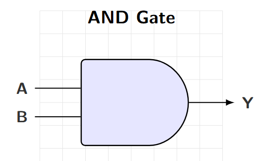
AND Gate
Properties
-
Output HIGH only when ALL inputs are HIGH
-
Boolean Expression: \(Y = A \cdot B\)
-
Also written as: \(Y = A \text{ AND } B\)
Applications :
-
Enable/Disable circuits
-
Multiplication in binary
-
Control logic
Truth Table
| A | B | Y |
|---|---|---|
| 0 | 0 | 0 |
| 0 | 1 | 0 |
| 1 | 0 | 0 |
| 1 | 1 | 1 |
Logic Symbol
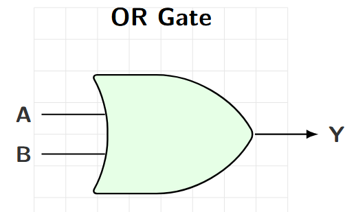
OR Gate
Properties
-
Output HIGH when AT LEAST ONE input is HIGH
-
Boolean Expression: \(Y = A + B\)
-
Also written as: \(Y = A \text{ OR } B\)
Applications :
-
Multiple input selection
-
Addition in binary
-
Alarm systems
Truth Table
| A | B | Y |
|---|---|---|
| 0 | 0 | 0 |
| 0 | 1 | 1 |
| 1 | 0 | 1 |
| 1 | 1 | 1 |
Logic Symbol
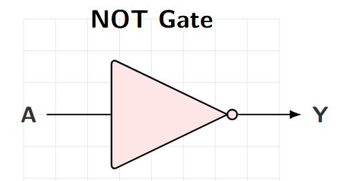
NOT Gate (Inverter)
Properties
-
Output is COMPLEMENT of input
-
Boolean Expression: \(Y = \overline{A}\)
-
Also written as: \(Y = \text{NOT } A\)
-
Single input gate
Applications :
-
Signal inversion
-
Complement generation
-
Buffer circuits
Truth Table
| A | Y |
|---|---|
| 0 | 1 |
| 1 | 0 |
Logic Symbol
Derived Logic Gates
NAND, NOR, XOR, XNOR
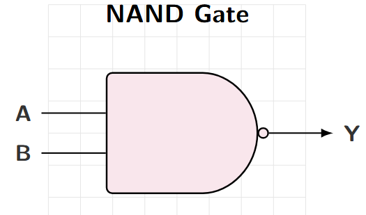
NAND Gate (NOT-AND)
Properties
-
Output LOW only when ALL inputs are HIGH
-
Boolean Expression: \(Y = \overline{A \cdot B}\)
-
Complement of AND gate
-
Universal Gate
Key Point :
-
Most commonly used gate in digital ICs
-
Easiest to manufacture
Truth Table
| A | B | Y |
|---|---|---|
| 0 | 0 | 1 |
| 0 | 1 | 1 |
| 1 | 0 | 1 |
| 1 | 1 | 0 |
Logic Symbol
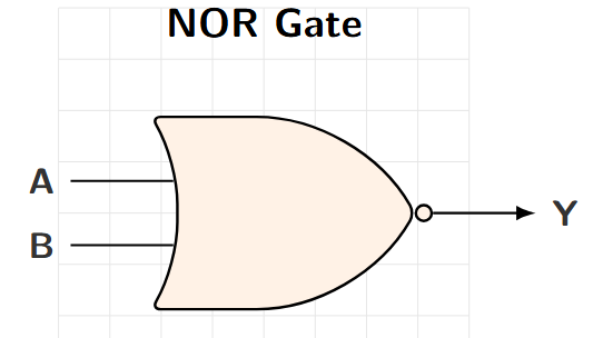
NOR Gate (NOT-OR)
Properties
-
Output HIGH only when ALL inputs are LOW
-
Boolean Expression: \(Y = \overline{A + B}\)
-
Complement of OR gate
-
Universal Gate
Applications :
-
Used in certain IC families
-
Logic minimization
Truth Table
| A | B | Y |
|---|---|---|
| 0 | 0 | 1 |
| 0 | 1 | 0 |
| 1 | 0 | 0 |
| 1 | 1 | 0 |
Logic Symbol
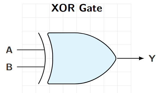
XOR Gate (Exclusive-OR)
Properties
-
Output HIGH when inputs are DIFFERENT
-
Boolean Expression: \(Y = A \oplus B\)
-
Also: \(Y = A\overline{B} + \overline{A}B\)
Applications :
-
Comparison circuits
-
Parity generators
-
Adder circuits
-
Error detection
Truth Table
| A | B | Y |
|---|---|---|
| 0 | 0 | 0 |
| 0 | 1 | 1 |
| 1 | 0 | 1 |
| 1 | 1 | 0 |
Logic Symbol
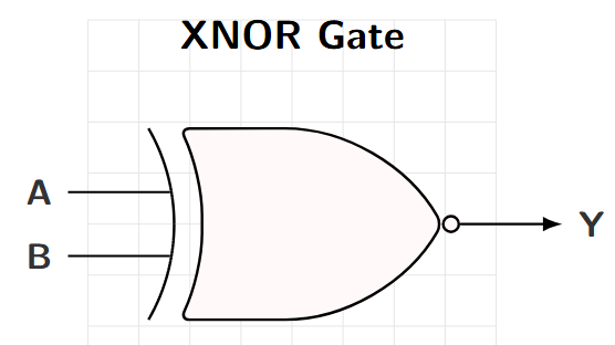
XNOR Gate (Exclusive-NOR)
Properties
-
Output HIGH when inputs are SAME
-
Boolean Expression: \(Y = \overline{A \oplus B}\)
-
Also: \(Y = AB + \overline{A}\,\overline{B}\)
-
Complement of XOR
Applications :
-
Equality comparators
-
Parity checkers
-
Code converters
Truth Table
| A | B | Y |
|---|---|---|
| 0 | 0 | 1 |
| 0 | 1 | 0 |
| 1 | 0 | 0 |
| 1 | 1 | 1 |
Logic Symbol
Universal Gates
Why Universal Gates?
What Makes a Gate Universal?
-
Definition : A gate that can implement ANY Boolean function
-
Requirement : Must be able to realize AND, OR, and NOT operations
-
Universal Gates : NAND and NOR
Advantages of Universal Gates :
-
Simplified Manufacturing : Only one type of gate needed
-
Cost Reduction : Bulk production of single gate type
-
Design Simplification : Uniform circuit design
-
Reduced Inventory : Fewer gate types to stock
Industry Impact :
-
Most digital ICs use NAND gates internally
-
TTL and CMOS families primarily based on NAND/NOR
NAND as Universal Gate
NAND Gate Implementations
Implementing Basic Gates using NAND :
-
NOT Gate :
\[\overline{A} = \text{NAND}(A, A) = \overline{A \cdot A} = \overline{A}\] -
AND Gate :
\[A \cdot B = \overline{\overline{A \cdot B}} = \text{NAND}(\text{NAND}(A, B), \text{NAND}(A, B))\] -
OR Gate (Using De Morgan's Law):
\[A + B = \overline{\overline{A} \cdot \overline{B}} = \text{NAND}(\text{NAND}(A, A), \text{NAND}(B, B))\]
Key Insight : Any Boolean expression can be converted to use only NAND gates by:
-
Converting to sum-of-products form
-
Applying De Morgan's laws
-
Using double negation
NAND Implementation Example
Example : Implement \(F = A \cdot B + C\) using only NAND gates
Step-by-Step Process :
-
Start with: \(F = A \cdot B + C\)
-
Apply double negation: \(F = \overline{\overline{A \cdot B + C}}\)
-
Use De Morgan's: \(F = \overline{\overline{A \cdot B} \cdot \overline{C}}\)
-
Express in NAND form: \(F = \text{NAND}(\text{NAND}(A, B), \text{NAND}(C, C))\)
Required NAND Gates :
-
Gate 1: \(\text{NAND}(A, B)\) produces \(\overline{A \cdot B}\)
-
Gate 2: \(\text{NAND}(C, C)\) produces \(\overline{C}\)
-
Gate 3: \(\text{NAND}(\text{Gate 1 output}, \text{Gate 2 output})\) produces \(F\)
Total : 3 NAND gates required
NOR as Universal Gate
NOR Gate Implementations
Implementing Basic Gates using NOR :
-
NOT Gate :
\[\overline{A} = \text{NOR}(A, A) = \overline{A + A} = \overline{A}\] -
OR Gate :
\[A + B = \overline{\overline{A + B}} = \text{NOR}(\text{NOR}(A, B), \text{NOR}(A, B))\] -
AND Gate (Using De Morgan's Law):
\[A \cdot B = \overline{\overline{A} + \overline{B}} = \text{NOR}(\text{NOR}(A, A), \text{NOR}(B, B))\]
Conversion Strategy for NOR :
-
Convert Boolean expression to product-of-sums form
-
Apply De Morgan's laws
-
Use double negation principle
Logic Circuit Realization
Design Process
Logic Circuit Design Process
Step-by-Step Design Methodology :
-
Problem Analysis :
-
Understand the problem statement
-
Identify inputs and outputs
-
Determine the required logic function
-
-
Truth Table Construction :
-
List all possible input combinations
-
Determine corresponding outputs
-
Verify logic requirements
-
-
Boolean Expression Derivation :
-
Write sum-of-products (SOP) or product-of-sums (POS)
-
Simplify using Boolean algebra or K-maps
-
-
Circuit Implementation :
-
Choose appropriate gates
-
Draw the logic circuit
-
Verify the design
-
Practical Example
Complete Design Example
Problem : Design a circuit for a 2-input majority function
Requirements : Output should be HIGH when majority of inputs are HIGH
Truth Table
| A | B | F |
|---|---|---|
| 0 | 0 | 0 |
| 0 | 1 | 0 |
| 1 | 0 | 0 |
| 1 | 1 | 1 |
Boolean Expression
Circuit : Simple AND Gate
Verification :
-
When A=0, B=0: \(F = 0 \cdot 0 = 0\) \(\checkmark\)
-
When A=0, B=1: \(F = 0 \cdot 1 = 0\) \(\checkmark\)
-
When A=1, B=0: \(F = 1 \cdot 0 = 0\) \(\checkmark\)
-
When A=1, B=1: \(F = 1 \cdot 1 = 1\) \(\checkmark\)
Complex Example: Three-Input Function
Problem : Implement \(F = AB + \overline{C}(A + B)\)
Step 1 : Expand the expression
Step 2 : Truth table verification
| A | B | C | AB | A \(\overline{\textbf{C}}\) | B \(\overline{\textbf{C}}\) | F |
|---|---|---|---|---|---|---|
| 0 | 0 | 0 | 0 | 0 | 0 | 0 |
| 0 | 0 | 1 | 0 | 0 | 0 | 0 |
| 0 | 1 | 0 | 0 | 0 | 1 | 1 |
| 0 | 1 | 1 | 0 | 0 | 0 | 0 |
| 1 | 0 | 0 | 0 | 1 | 0 | 1 |
| 1 | 0 | 1 | 0 | 0 | 0 | 0 |
| 1 | 1 | 0 | 1 | 1 | 1 | 1 |
| 1 | 1 | 1 | 1 | 0 | 0 | 1 |
Implementation with Universal Gates
Implementing with NAND Gates Only
Example : Convert \(F = AB + \overline{C}\) to NAND-only implementation
Method 1 - Direct Conversion :
-
\(F = AB + \overline{C}\)
-
Apply double negation: \(F = \overline{\overline{AB + \overline{C}}}\)
-
Use De Morgan's: \(F = \overline{\overline{AB} \cdot \overline{\overline{C}}}\)
-
Simplify: \(F = \overline{\overline{AB} \cdot C}\)
-
NAND form: \(F = \text{NAND}(\text{NAND}(A,B), C)\)
Required Gates :
-
NAND Gate 1: Inputs A, B \(\to\) Output \(\overline{AB}\)
-
NAND Gate 2: Inputs (Gate 1 output), C \(\to\) Output F
Gate Count : 2 NAND gates
Practical Considerations
IC Families and Gate Selection
Common Logic Families :
-
TTL (Transistor-Transistor Logic) :
-
74xx series (e.g., 7400 - Quad 2-input NAND)
-
Fast switching, moderate power consumption
-
Voltage: +5V supply
-
-
CMOS (Complementary Metal-Oxide Semiconductor) :
-
74HCxx, 74ACxx series
-
Very low power consumption
-
Wide supply voltage range: 3V to 15V
-
-
ECL (Emitter-Coupled Logic) :
-
Highest speed operation
-
High power consumption
-
Used in specialized applications
-
Selection Criteria :
-
Speed requirements
-
Power consumption constraints
-
Voltage compatibility
-
Cost considerations
Design Guidelines and Best Practices
Circuit Design Guidelines :
-
Minimize Gate Count :
-
Use Boolean simplification techniques
-
Consider using universal gates for uniformity
-
Avoid redundant logic paths
-
-
Consider Propagation Delay :
-
Each gate introduces delay (typically 1-20 ns)
-
Minimize logic levels for faster operation
-
Use parallel paths where possible
-
-
Power Considerations :
-
CMOS gates consume power only during switching
-
TTL gates have constant current draw
-
Consider fan-out limitations
-
-
Noise Immunity :
-
Maintain proper voltage levels
-
Use appropriate decoupling capacitors
-
Minimize wire lengths for high-speed signals
-
Advanced Topics
Multi-Input Gates
Extending to Multiple Inputs :
-
3-Input AND Gate : \(Y = A \cdot B \cdot C\)
-
Output HIGH only when ALL three inputs are HIGH
-
Can be cascaded from 2-input gates: \(Y = (A \cdot B) \cdot C\)
-
-
4-Input NAND Gate : \(Y = \overline{A \cdot B \cdot C \cdot D}\)
-
Output LOW only when ALL four inputs are HIGH
-
Commonly available in IC packages
-
-
8-Input OR Gate : \(Y = A + B + C + D + E + F + G + H\)
-
Output HIGH when ANY input is HIGH
-
Can be built using tree structure of 2-input gates
-
Practical Implementation :
-
Use cascaded 2-input gates
-
Consider available IC packages
-
Optimize for speed vs. gate count
Wired Logic and Open-Collector Gates
Wired-AND Logic :
-
Concept : Multiple open-collector outputs connected together
-
Function : Acts as AND operation without additional gates
-
Application : Bus systems, interrupt lines
Advantages :
-
Reduced gate count
-
Simple bus implementation
-
Easy expansion of logic
Considerations :
-
Requires pull-up resistors
-
Slower switching due to RC time constants
-
Limited to specific logic families
Example Applications :
-
Computer data buses
-
Interrupt request lines
-
Multi-master communication systems
Problem Solving Techniques
Systematic Problem Solving
Approach for Complex Logic Problems :
-
Problem Understanding :
-
Read the problem statement carefully
-
Identify all inputs and outputs
-
Understand the functional requirements
-
-
Truth Table Method :
-
List all possible input combinations
-
Determine the desired output for each combination
-
Use this to derive the Boolean expression
-
-
Boolean Algebra Simplification :
-
Apply Boolean laws and theorems
-
Use Karnaugh maps for systematic simplification
-
Verify the simplified expression
-
-
Implementation Choice :
-
Choose between different gate types
-
Consider using universal gates
-
Optimize for the given constraints
-
Common Mistakes and How to Avoid Them
Frequent Student Errors :
-
Truth Table Errors :
-
Mistake : Missing input combinations
-
Solution : Systematically list all \(2^n\) combinations
-
-
Boolean Expression Mistakes :
-
Mistake : Incorrect operator precedence
-
Solution : Use parentheses to clarify precedence
-
-
Gate Symbol Confusion :
-
Mistake : Mixing up NAND and NOR symbols
-
Solution : Remember the bubble indicates inversion
-
-
Universal Gate Implementation :
-
Mistake : Incorrect application of De Morgan's laws
-
Solution : Apply double negation systematically
-
Verification Strategy : Always check your final circuit against the original truth table
Real-World Applications
Logic Gates in Digital Systems
Computer Systems :
-
CPU Design : ALU operations, control units
-
Memory Systems : Address decoders, read/write control
-
I/O Interfaces : Data routing, protocol handling
Communication Systems :
-
Error Detection : Parity checkers using XOR gates
-
Data Encoding : Manchester encoding, scrambling
-
Protocol Processing : Frame detection, data validation
Control Systems :
-
Industrial Automation : PLC programming, safety interlocks
-
Automotive Electronics : Engine control, safety systems
-
Home Automation : Smart switches, sensor integration
Consumer Electronics :
-
Digital Cameras : Image processing, compression
-
Mobile Phones : Signal processing, user interface
-
Gaming Consoles : Graphics processing, input handling
Emerging Applications
Modern Applications :
-
Internet of Things (IoT) :
-
Sensor data processing
-
Low-power logic design
-
Wireless communication protocols
-
-
Artificial Intelligence Hardware :
-
Neural network accelerators
-
Specialized logic for AI computations
-
Parallel processing architectures
-
-
Quantum Computing Interfaces :
-
Classical-quantum signal conversion
-
Error correction systems
-
Control signal generation
-
-
Biomedical Devices :
-
Pacemaker control logic
-
Medical imaging systems
-
Patient monitoring equipment
-
Summary and Review
Key Concepts Review
Essential Points to Remember :
-
Basic Gates : AND, OR, NOT are fundamental building blocks
-
Derived Gates : NAND, NOR, XOR, XNOR extend functionality
-
Universal Gates : NAND and NOR can implement any logic function
-
Design Process : Truth table \(\to\) Boolean expression \(\to\) Circuit
-
Practical Considerations : IC families, power, speed, cost
Problem-Solving Skills Developed :
-
Truth table construction and analysis
-
Boolean expression manipulation
-
Circuit design and optimization
-
Universal gate implementation techniques
Next Topics :
-
Combinational logic circuits (adders, multiplexers, decoders)
-
Sequential logic circuits (flip-flops, counters, registers)
Practice Problems
Problems for Self-Study :
-
Implement \(F = ABC + \overline{A}BC + A\overline{B}C\) using:
-
Basic gates (AND, OR, NOT)
-
Only NAND gates
-
Only NOR gates
-
-
Design a 3-input majority function using minimum number of gates
-
Convert the following to NAND-only implementation:
\[F = (A + B)(C + D)\] -
Prove that XOR gate can be implemented using 4 NAND gates
-
Design a logic circuit that outputs HIGH when exactly two out of three inputs are HIGH
Verification : Always verify your solutions using truth tables
Key Takeaways :
-
Logic gates are the foundation of digital electronics
-
Universal gates provide design flexibility and cost benefits
-
Systematic design approach ensures correct implementations
-
Understanding applications helps appreciate the relevance