Overview
Demonstrative Video
Need for a Diode - Initial Thoughts
-
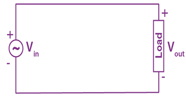
Charger Circuit Operation
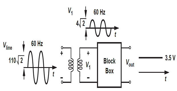
\(\xrightarrow[\text{110 V}]{\text{ac voltage}}\) \(\xrightarrow[\text{4 V}]{\text{Transformer}}\) \(\xrightarrow[\text{3.5 V}]{\text{dc voltage using LPF}}\)
-
Output of TF using black box exhibits a zero dc content as -ve and +ve half cycles enclose equal areas, leading to a zero average


DIODE - Basic Ideas
-
Resistor \(\rightarrow\) linear device \(\rightarrow\) current Vs voltage is a straight line.
-
Diode \(\rightarrow\) nonlinear device \(\rightarrow\) \(I\) Vs \(V\) is not a straight line.
-
The reason is the barrier potential.
-
A pn junction is known as a semiconductor diode.
-
Also known as crystal diodes since grown out of a crystal (like Ge/ Si).
-
A diode has two terminals.
-
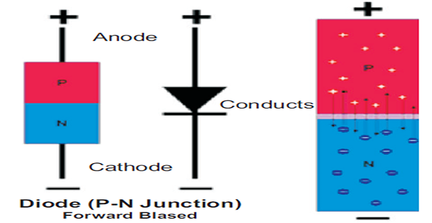
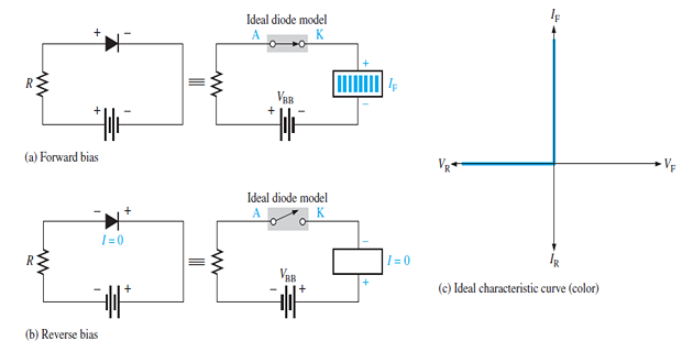
Conducts only when forward biased, i.e., when the terminal connected with the arrowhead is at a higher potential than the terminal connected to the bar.
-
When reverse biased, practically does not conduct any current through it.
-
A region around the junction from which the charge carriers (free electrons and holes) are depleted called the depletion layer .
-
A potential difference built up across the pn junction, which restricts further movement of charge carriers across the junction, known as potential barriers .
-
When a pn junction is connected across an electric supply (potential difference), the junction is said to be under biasing .

-
Forward Biasing
-
When positive terminal of DC source or battery is connected to the p-type semiconductor and the negative terminal is connected to the n-type semiconductor of a pn junction, the junction is said to be in forward biasing.
-
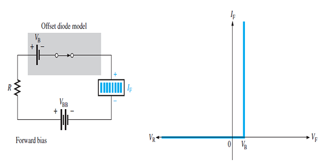
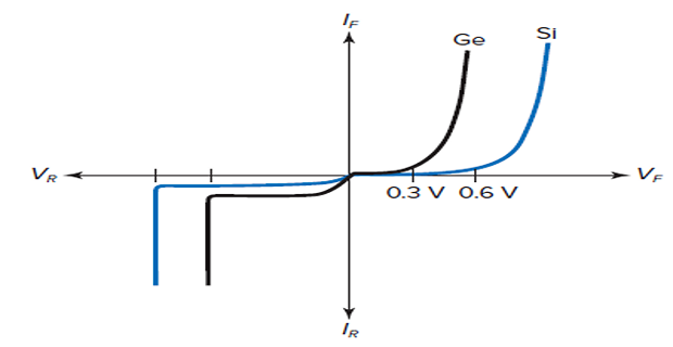
The junction potential barrier is reduced , and at some forward voltage (0.3 V for Ge and 0.7 V for Si), it is eliminated altogether.
-
The junction offers low resistance to the flow of current through it.
-
The current magnitude through the circuit depends upon the applied forward voltage.
-
-
Reverse Biasing
-
When the positive terminal is connected to the n-type semiconductor and the negative terminal is connected to the p-type semiconductor of a pn junction, the junction is said to be in reverse biasing.
-
The junction potential barrier is strengthened .
-
The junction offers high resistance to the flow of current through it.
-
The current magnitude through the circuit depends upon the applied reverse voltage.
-


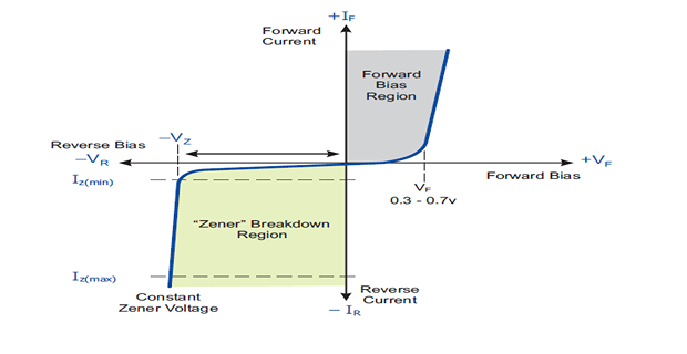
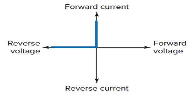
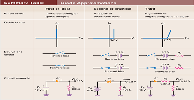
Ideal Diode: acts like a perfect conductor (zero resistance) when forward biased and like a perfect insulator ( \(\infty\) resistance) when reverse biased.
Diode Characteristic Curve

Real
diode
Ideal
diode
Si Vs
Ge
-
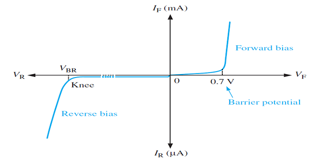
Above the knee voltage, the diode current increases rapidly.
-
Small increase in the diode voltage cause large increases in diode current.
-
. is less than 1 depends on the size of the p and n regions and how heavily doped they are. Often, Bulk Resistance :\[\text{Bulk resistance}~R_B = R_p + R_n\]
-
Maximum DC Forward Current : If the current in a diode is too large, the excessive heat can destroy the diode. The \(I_{F(max)}\) is one of the maximum ratings given on a data sheet.
-
The power rating is the maximum power the diode can safely dissipate without shortening its life or degrading its properties Power Dissipation :\[\begin{aligned} P_D & = V_D \cdot I_D \\ P_{max} & = V_{max} \cdot I_{max} \end{aligned}\]
Diode Current Equation
-
When the diode is reverse biased, its current equation may be obtained by changing the sign of the applied voltage \(V\) .
-
Thus, the diode current with reverse bias is\[I=I_o\left[\mathrm{e}^{\left(-V / \eta V_T\right)}-1\right]\]
-
If \(V \gg V_T\) , then the term \(\mathrm{e}^{\left(-V / \eta v_T\right)} \ll 1\) , therefore \(I \approx-I_o\) , termed as reverse saturation current , which is valid as long as the external voltage is below the breakdown value.
Load Lines
-
Load line\[I_D=\frac{V_S-V_D}{R_s}\]


-
If \(V_s = 2~\mathrm{V}\) , \(R = 100~\Omega\)
-
\(V_D = 0 \Rightarrow I_D = 20~\mathrm{mA}\)
-
\(I_D = 0 \Rightarrow V_D = V_s = 2~\mathrm{V}\)
-
The straight line is called the load line
-
\(Q\) is an abbreviation for quiescent , which means “at rest.”
Problem-1
-
A germanium PN junction diode is forward biased with a voltage of 0.7 V applied across it. The diode has a saturation current of 10 \(\mu\) A and a forward bias resistance of 50 \(\Omega\) . Calculate the current flowing through the diode if the thermal voltage is 26 mV.
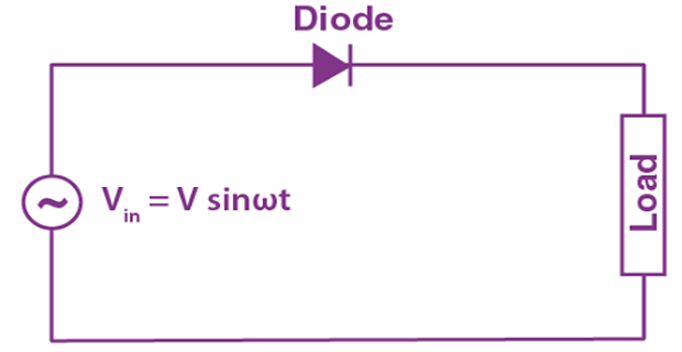
Diode as a Rectifiers
-
Electrical power generated T & D as a.c. for economical reasons.
-
The alternating voltage is available at the mains but most of the electronic circuit need d.c. voltage for their operation.
-
Therefore the rectifier is needed to convert ac to dc.
-
The rectifier can be of two types:
-
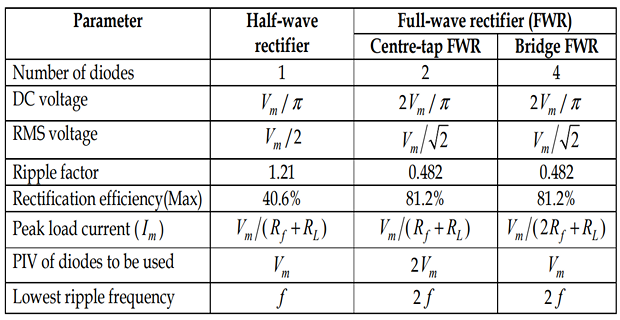
Half-Wave Rectifier
-
Full-Wave Rectifier
-
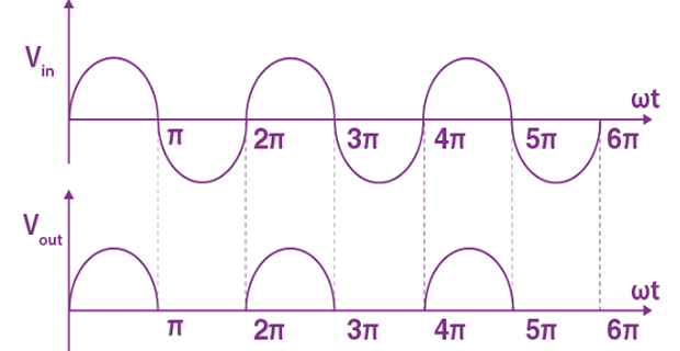
Half-Wave Rectifiers
-
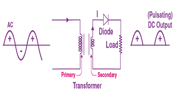
A half-wave rectifier is a simple electronic circuit that converts an alternating current (AC) input signal into a pulsating direct current (DC) output signal. It uses a diode as its main component.
Operation:
-
The AC input signal is applied to the primary side of a step-down transformer to reduce the voltage to a suitable level.
-
The transformed AC voltage is then applied to the diode, which acts as a one-way valve for electric current.
-
During the positive half-cycle of the AC input, the diode conducts and allows the current to flow through it, resulting in a positive voltage across the load resistor.
-
During negative half-cycle of AC input, diode becomes reverse-biased and blocks the current flow. Hence, no voltage is present across the load resistor during this period.
-
The output waveform of the rectifier is a pulsating DC voltage that only contains the positive half-cycles of the input signal.
Forward-Biased
Reverse-Biased

Important formulas
-
Peak voltage (Vp): \(V_p = \dfrac{V_m}{\sqrt{2}}\)
-
Average voltage (Vavg): \(V_{\text{avg}} = \dfrac{V_p}{\pi}\)
-
Peak-to-Peak voltage (Vpp): \(V_{\text{pp}} = 2 \cdot V_p\)
-
RMS voltage (Vrms): \(V_{\text{rms}} = \dfrac{V_p}{\sqrt{2}}\)
-
Rectification Efficiency ( \(\eta\) ): \(\eta = \dfrac{V_{\text{avg}}}{V_{\text{rms}}} \times 100\%\)
Full-wave rectifiers
-
Significant power is lost while using a half-wave rectifier.
-
Full wave rectifiers provide a smooth and steady supply of power.
-
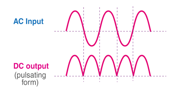
A full wave rectifier converts the complete cycle of alternating current into pulsating DC.
-
Full wave rectifiers utilize the full cycle of the input AC.
-
There are two methods to construct a full wave rectifier:
-
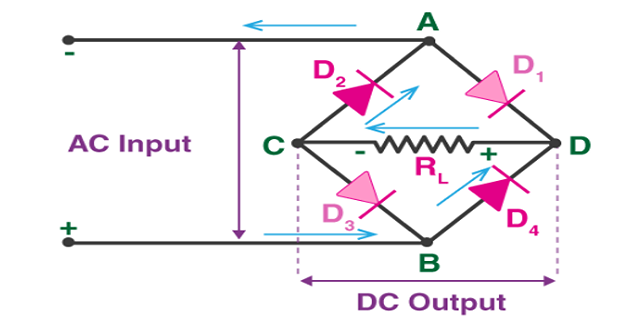
Centre tapped rectifiers: Uses a centre tapped transformer and two diodes.
-
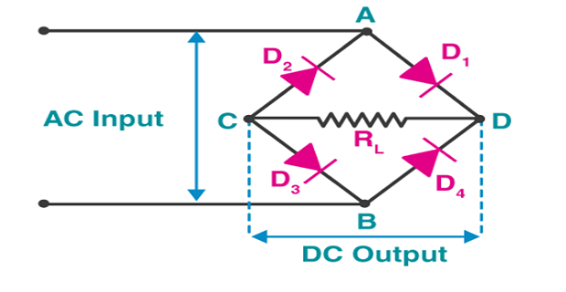
Bridge rectifier: Uses a standard transformer with four diodes arranged as a bridge.
-
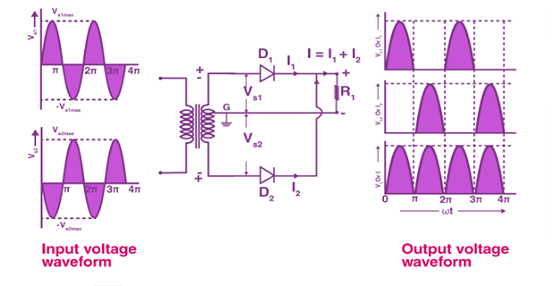
Centre-tapped Full-Wave Rectifiers
-
Consists of a centre tapped step-down TF and two diodes.
-
The output voltage is obtained across the connected load resistor.
-
The step-down TF converts the HV AC into LV AC.
-
During the positive half cycle, diode D1 conducts as a short circuit while D2 acts as an open circuit.
-
During the negative half cycle, diode D1 acts as an open circuit while D2 conducts as a short circuit.
-
DC voltage is obtained for both positive and negative half cycles.
Bridge Rectifiers

Important Formulas
-
Peak Inverse Voltage :
-
maximum voltage a diode can withstand in the reverse-biased direction before breakdown.
-
The PIV of the full-wave rectifier is double that of a half-wave rectifier.
-
The PIV across D1 and D2 is \(2V_{\text{max}}\)
-
-
DC Output Voltage : \(V_{dc} = I_{avg}R_{L} = \dfrac{2}{\pi}I_{max}R_L\)
-
RMS Current : \(I_{rms} =\dfrac{I_{max}}{\sqrt{2}}\)
-
Rectification efficiency : \(\eta = \dfrac{\text{DC output power}}{\text{AC output power}}\)
Ripples in Rectified DC Output
-
Ripple refers to small fluctuations in the output voltage or current of a rectifier circuit.
-
It is caused by the pulsating nature of the rectified waveform.
-
The rectified waveform consists of positive and negative half cycles.
-
During the transition between half cycles, there is a brief period where the voltage or current decreases or crosses zero.
-
This transition period leads to fluctuations in the output, resulting in a ripple component superimposed on the DC signal.
-
Ripple is typically expressed as the peak-to-peak value or the root mean square (RMS) value of the fluctuation.
-
It is undesirable in applications requiring a steady and smooth DC voltage or current.
-
Ripple can cause distortions or malfunctions in sensitive electronic components.
-
Additional filtering or regulation techniques can be used to reduce the ripple and obtain a more stable DC output.
Summary
Problem-1
-
An a.c. supply of 230 V is applied to a half-wave rectifier circuit through a transformer of turn ratio 10:1. Find (i) the output d.c. voltage and (ii) the peak inverse voltage. Assume the diode to be ideal.

Problem-2
-
A crystal diode having internal resistance \(R_f = 20~\Omega\) is used for half-wave rectification. If the applied voltage \(v = 50 \sin \omega t\) and load resistance \(R_L= 800~\Omega\) , find : (i) \(I_m\) , \(I_{dc}\) , \(I_{rms}\) (ii) a.c. power input and d.c. power output (iii) d.c. output voltage (iv) efficiency of rectification.
Problem-3
A half-wave rectifier is used to supply \(50 ~\mathrm{~V}\) d.c. to a resistive load of \(800~ \Omega\) . The diode has a resistance of \(25~ \Omega\) . Calculate a.c. voltage required.
Problem-4
A full-wave rectifier uses two diodes, the internal resistance of each diode may be assumed constant at \(20~ \Omega\) . The transformer r.m.s. secondary voltage from centre tap to each end of secondary is \(50~ \mathrm{~V}\) and load resistance is \(980~ \Omega\) . Find : (i) the mean load current (ii) the r.m.s. value of load current.
Problem-5
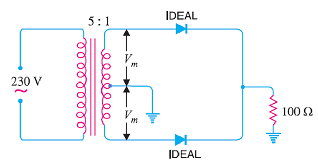
-
In the centre-tap circuit, the diodes are assumed to be ideal i.e. having zero internal resistance. Find :(i) d.c. output voltage(ii) peak inverse voltage (iii) rectification efficiency.