Demonstrative Video
\(\bullet\) Transformer with resistance and leakage reactance
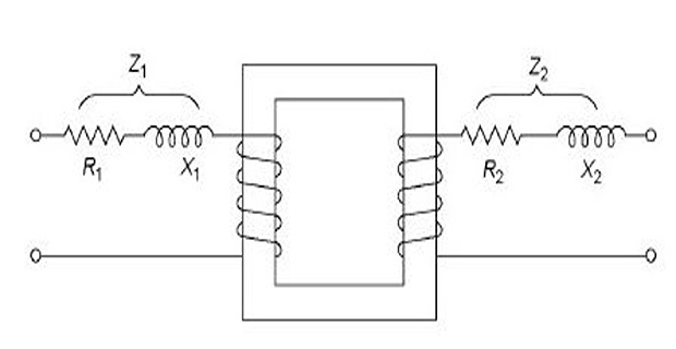
\[\begin{aligned}
Z_{1} & =\sqrt{\left(R_{1}^{2}+X_{1}^{2}\right)}\\
Z_{2} & =\sqrt{\left(R_{2}^{2}+X_{2}^{2}\right)}\\
V_{1} & =E_{1}+I_{1}\left(R_{1}+jX_{1}\right)=E_{1}+I_{1}Z_{1}\\
E_{2} & =V_{2}+I_{2}\left(R_{2}+jX_{2}\right)=V_{2}+I_{2}Z_{2}
\end{aligned}\]
\[\begin{array}{ccc}
X_{2}^{'}=X_{2}/K^{2} & \mbox{and} &
X_{1}^{'}=K^{2}X_{1}\\
X_{01}=X_{1}+X_{2}^{'} & \mbox{and} &
X_{02}=X_{2}+X_{1}^{'}
\end{array}\]
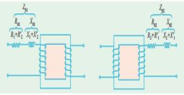
\[\begin{aligned}
Z_{01} & =\sqrt{\left(R_{01}^{2}+X_{01}^{2}\right)}\\
Z_{02} & =\sqrt{\left(R_{02}^{2}+X_{02}^{2}\right)}
\end{aligned}\]
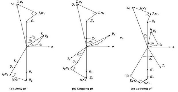
Voltage Drop in a Transformer
\[\begin{aligned}
V_{1} & \thickapprox E_{1}\\
E_{2} & =KE_{1}=KV_{1}\\
E_{2} & =_{0}V_{2}
\end{aligned}\]
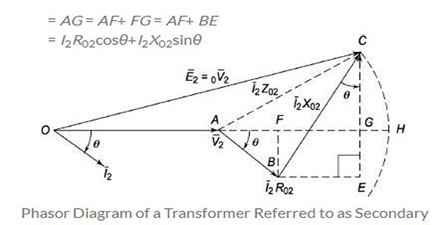
\[I_{2}R_{02}\cos\Phi\pm
I_{2}X_{02}\sin\Phi\]
\[I_{1}R_{01}\cos\Phi\pm
I_{1}X_{01}\sin\Phi\]
\[\begin{aligned}
v_{r} &
=\dfrac{I_{2}R_{02}}{_{0}V_{2}}\times100=\dfrac{I_{1}R_{01}}{V_{1}}\times100=\mbox{percentage
resistive drop}\\
v_{x} &
=\dfrac{I_{2}X_{02}}{_{0}V_{2}}\times100=\dfrac{I_{1}X_{01}}{V_{1}}\times100=\mbox{percentage
reactive drop}
\end{aligned}\]
\[\begin{aligned}
= & \dfrac{I_{2}R_{02}cos\Phi\pm
I_{2}X_{02}sin\Phi}{_{0}V_{2}}\times100\\
= & v_{r}cos\Phi\pm v_{x}sin\Phi
\end{aligned}\]
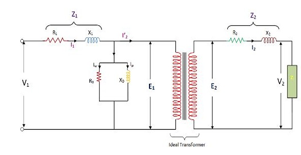
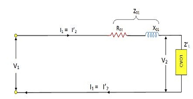
Equivalent Circuit of a Transformer
Equivalent circuit is basically a diagram in which the resistance and leakage reactance of the transformer are imagined to be external to the winding
The equivalent circuit diagram of transformer is given below:-
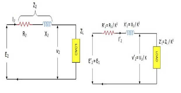
The secondary circuit and its equivalent primary value
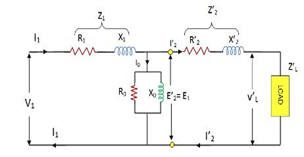
The total equivalent circuit is obtained by adding in the primary impedance
It can be simplified
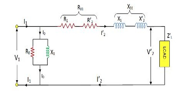
At last, the circuit is simplified by omitting \(I_0\) altogether
\[\begin{aligned}
Z &
=Z_{1}+Z_{m}||\left(Z_{2}^{'}+Z_{L}^{'}\right)\\
&
=Z_{1}+\dfrac{Z_{m}\left(Z_{2}^{'}+Z_{L}^{'}\right)}{Z_{m}+\left(Z_{2}^{'}+Z_{L}^{'}\right)}
\end{aligned}\]
\[V_{1}=I_{1}\left[Z_{1}+\dfrac{Z_{m}\left(Z_{2}^{'}+Z_{L}^{'}\right)}{Z_{m}+\left(Z_{2}^{'}+Z_{L}^{'}\right)}\right]\]