SECTION 01
Bus Admittance Matrix
The meeting point of various components in a PS is called
Bus.
The Bus or Bus bar is a conductor made of copper or aluminium
having negligible resistances.
Hence the bus bar will have zero voltage drop when it conducts
the rated current
Buses are considered as points of constant voltage in a
PS
PS represented by impedance/reactance diagram is considered as a
circuit or network.
Buses can be treated as nodes and the voltages of all buses
(nodes) can be solved by conventional node analysis technique.
\[\mathrm{Y_{bus}}\cdot \mathrm{V} =
\mathrm{I}\]
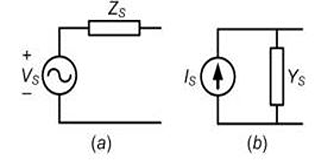
will be
+ve will be
-ve and Note: If PS represented by reactance
diagram, all elements are inductive susceptances (which are -ve). In
this case, In general, where,
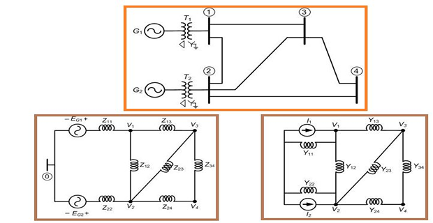
A simple power system with impedance and admittance diagram
\[\left[\begin{array}{c}
I_{1}\\
I_{2}\\
0\\
0
\end{array}\right]=Y_{bus}\left[\begin{array}{c}
V_{1}\\
V_{2}\\
V_{3}\\
V_{4}
\end{array}\right]\Longrightarrow\left[\begin{array}{c}
V_{1}\\
V_{2}\\
V_{3}\\
V_{4}
\end{array}\right]=Z_{bus}\left[\begin{array}{c}
I_{1}\\
I_{2}\\
0\\
0
\end{array}\right]\]
\[\begin{aligned}
I_{1} &
=Y_{11}V_{1}+Y_{12}\left(V_{1}-V_{2}\right)+Y_{13}\left(V_{1}-V_{3}\right)\\
& =\left(Y_{11}+Y_{12}+Y_{13}\right)V_{1}-Y_{12}V_{2}-Y_{13}V_{3}
\end{aligned}\]
Applying KCL at node 1,
\[\begin{aligned}
I_{2} &
=Y_{22}V_{2}+Y_{12}\left(V_{2}-V_{1}\right)+Y_{23}\left(V_{2}-V_{3}\right)+Y_{24}\left(V_{2}-V_{4}\right)\\
&
=-Y_{12}V_{1}+\left(Y_{22}+Y_{12}+Y_{23}+Y_{24}\right)V_{2}-Y_{23}V_{3}-Y_{24}V_{4}
\end{aligned}\]
In a similar way application of KCL at nodes 2, 3 and 4 results in
the following equations
\[\begin{aligned}
0 &
=Y_{13}\left(V_{3}-V_{1}\right)+Y_{23}\left(V_{3}-V_{2}\right)+Y_{34}\left(V_{3}-V_{4}\right)\\
&
=-Y_{13}V_{1}-Y_{23}V_{2}+\left(Y_{13}+Y_{23}+Y_{34}\right)V_{3}-Y_{34}V_{4}
\end{aligned}\]
\[\begin{aligned}
0 & =Y_{24}\left(V_{4}-V_{2}\right)+Y_{34}\left(V_{4}-V_{3}\right)\\
& =-Y_{24}V_{2}-Y_{34}V_{3}+\left(Y_{24}+Y_{34}\right)V_{4}
\end{aligned}\]
\[ \left[\begin{array}{c} I_{1}\\ I_{2}\\ 0\\ 0 \end{array}\right]=\left[\begin{array}{cccc} Y_{11}+Y_{12}+Y_{13} & -Y_{12} & -Y_{13} & 0\\ -Y_{12} & Y_{22}+Y_{12}+Y_{23}+Y_{24} & -Y_{23} &
-Y_{24}\\ -Y_{13} & -Y_{23} & Y_{13}+Y_{23}+Y_{34} & -Y_{34}\\ 0 & -Y_{24} & -Y_{34} & Y_{24}+Y_{34} \end{array}\right]\left[\begin{array}{c} V_{1}\\ V_{2}\\ V_{3}\\ V_{4} \end{array}\right] \]
On combining
\[ Y_{bus}=\left[\begin{array}{cccc} Y_{1}+Y_{12}+Y_{13} & -Y_{12} & -Y_{13} & 0\\ -Y_{12} & Y_{22}+Y_{12}+Y_{23}+Y_{24} & -Y_{23} &
-Y_{24}\\ -Y_{13} & -Y_{23} & Y_{13}+Y_{23}+Y_{34} & -Y_{34}\\ 0 & -Y_{24} & -Y_{34} & Y_{24}+Y_{34} \end{array}\right]=\left[\begin{array}{ccccc} Y_{11} & -Y_{12} & -Y_{13} & \cdots & -Y_{1n}\\ -Y_{12} & Y_{2} & -Y_{23} & \cdots & -Y_{2n}\\ \vdots & \vdots & \vdots & \ddots & \vdots\\ -Y_{1n} & -Y_{2n} & -Y_{3n} & \cdots & Y_{n} \end{array}\right] \]
SECTION 03
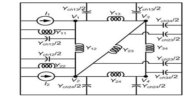
Inclusion of Line Charging Capacitors
Assume all lines are represented by equivalent-\(\pi\) with the shunt admittance between the
line \(i\) and \(j\) being denoted by \(Y_{chij}\)
Then equivalent admittance at the two end will be \(Y_{chij}/2\)
For e.g. shunt capacitance at two ends joining buses \(1\) and \(3\) will be \(Y_{ch13}/2\)
\[ Y_{bus}=\left[\begin{array}{cccc} Y_{1}+Y_{12}+Y_{13}+Y_{ch1} & -Y_{12} & -Y_{13} &
0\\ -Y_{12} & Y_{22}+Y_{12}+Y_{23}+Y_{24}+Y_{ch2} & -Y_{23}
& -Y_{24}\\ -Y_{13} & -Y_{23} & Y_{13}+Y_{23}+Y_{34}+Y_{ch3} &
-Y_{34}\\ 0 & -Y_{24} & -Y_{34} & Y_{24}+Y_{34}+Y_{ch4} \end{array}\right] \]
where \(\Rightarrow\)
SECTION 04
Some observation of\(Y_{bus}\)matrix
\(Y_{bus}\) is a sparse
matrix
Diagonal elements are dominating
Off diagonal elements are symmetric
The diagonal element of each node is the sum of the admittances
connected to it
The off diagonal element is negated admittance
\[ \left[\begin{array}{c} I_{1}\\ I_{2}\\ I_{3}\\ I_{4} \end{array}\right]=\underset{\mbox{symmetric}}{\underbrace{\left[\begin{array}{cccc} Y_{11} & Y_{12} & Y_{13} & Y_{14}\\ Y_{21} & Y_{22} & Y_{23} & Y_{24}\\ Y_{31} & Y_{32} & Y_{33} & Y_{34}\\ Y_{41} & Y_{42} & Y_{43} & Y_{44} \end{array}\right]}}\left[\begin{array}{c} V_{1}\\ V_{2}\\ V_{3}\\ V_{4} \end{array}\right]\Longrightarrow\left[\begin{array}{c} V_{1}\\ V_{2}\\ V_{3}\\ V_{4} \end{array}\right]=\underset{\mbox{symmetric}}{\underbrace{\left[\begin{array}{cccc} Z_{11} & Z_{12} & Z_{13} & Z_{14}\\ Z_{21} & Z_{22} & Z_{23} & Z_{24}\\ Z_{31} & Z_{32} & Z_{33} & Z_{34}\\ Z_{41} & Z_{42} & Z_{43} & Z_{44} \end{array}\right]}}\left[\begin{array}{c} I_{1}\\ I_{2}\\ I_{3}\\ I_{4} \end{array}\right] \]
\[Y_{11}={\left.\dfrac{I_{1}}{V_{1}}\right|}_{V_{2}=V_{3}=V_{4}=0}\]
\[Y_{12}={\left.\dfrac{I_{1}}{V_{2}}\right|}_{V_{1}=V_{3}=V_{4}=0}\]
\[Z_{11}={\left.\dfrac{V_{1}}{I_{1}}\right|}_{I_{2}=I_{3}=I_{4}=0}\]
\[Z_{12}={\left.\dfrac{V_{1}}{I_{2}}\right|}_{I_{1}=I_{3}=I_{4}=0}\]
NOTE: \(Z_{12}\) is not the
reciprocal of \(Y_{12}\)
SECTION 05
Node Elimination by Matrix Partitioning
\[\begin{aligned}
I_{A} & =KV_{A}+LV_{x}\\ I_{x} & =0=L^{T}V_{A}+MV_{x}\Rightarrow V_{x}=-M^{-1}L^{T}V_{A}\\ \therefore ~I_{A} & =\left(K-LM^{-1}L^{T}\right)V_{A}
\end{aligned}\]